Project 57

Project 57 is another CFA-based audio power amplifier project. The input stage is identical to previous CFA-based projects tied to a Complementary Feedback Pair (CFP) configured power output stage. A CFP circuit is also commonly known as a compound feedback pair or the Sziklai pair. Unlike the Darlington pair that uses the same type of transistors, the CFP consists of NPN and PNP transistors or vice versa. The main advantages of this type of circuit configuration are large beta gain and good linearity particularly in audio power amplifier applications, as verified and shown later in the project’s test results. Similarly, to make the project more interesting, the Vbe multiplier is also a Sziklai pair.
The CFP-based output stage circuit was first introduced in earlier LME49811-based power amplifier projects. However, this time it’s been modified for this project and surprisingly has proven its excellent audio quality and circuit performance. Because of the implemented CFP configuration, the prototype when tested requires only 1.075Vrms of 1KHz sinewave input signal to produce an unclipped output of about 41.66Vrms into an 8Ω load with ±64VDC power supply rails. This corresponds to a power output of about 217 watts or higher when connected to 4Ω loads.
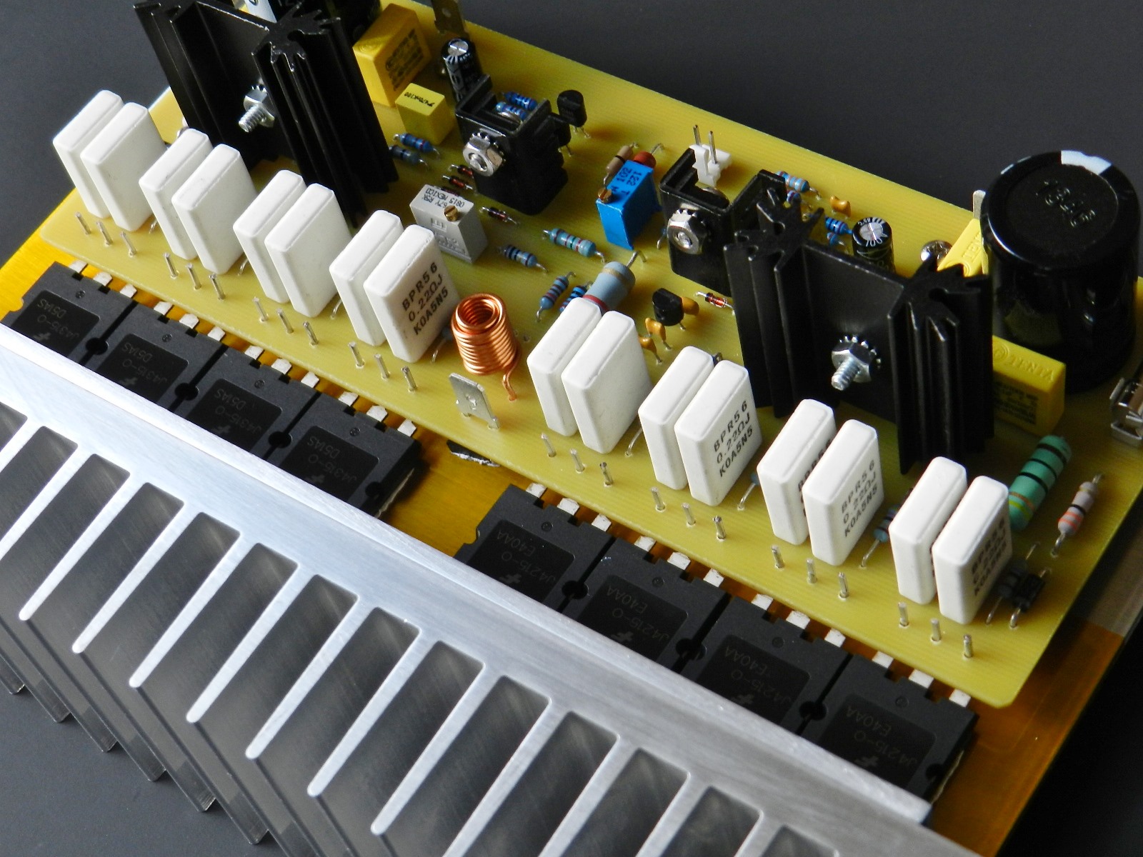
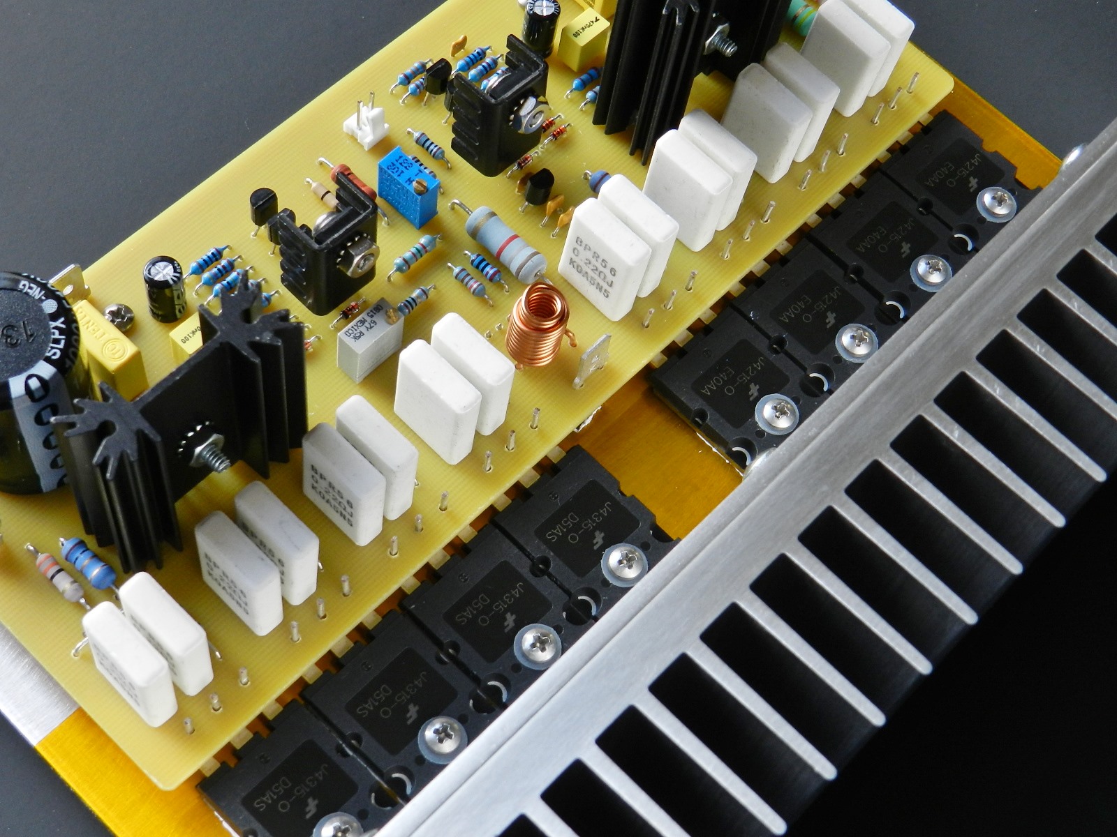
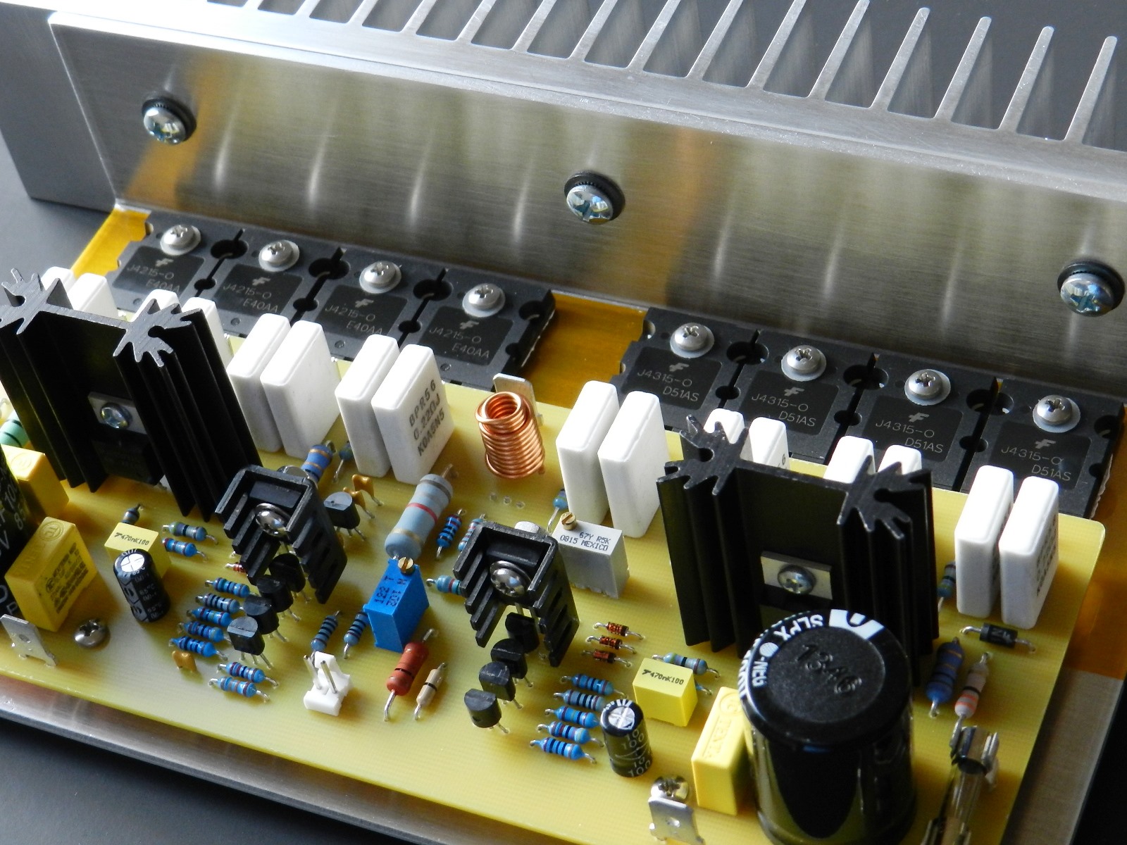
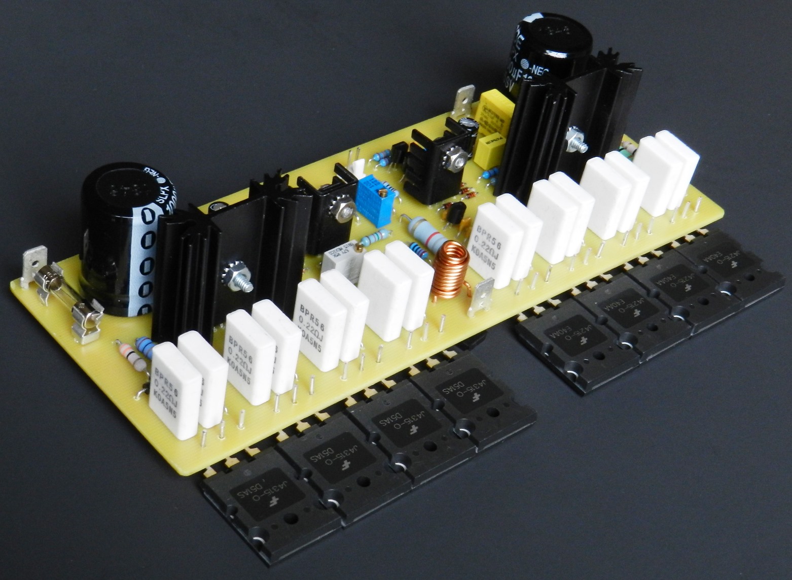
The TO264-packaged power output transistors from Fairchild Semiconductor have the same specifications as the popular 2SC5200/2SA1943, which are designed for excellent gain linearity in high-fidelity audio power amplifiers. All components listed in the Bill of Materials of the project are readily available standard parts. If you’re interested in building this project and have read the Information and Policies section of this website, the schematic diagram, PCB layout and BOM (available only by request) are free, as it is, no warranty.
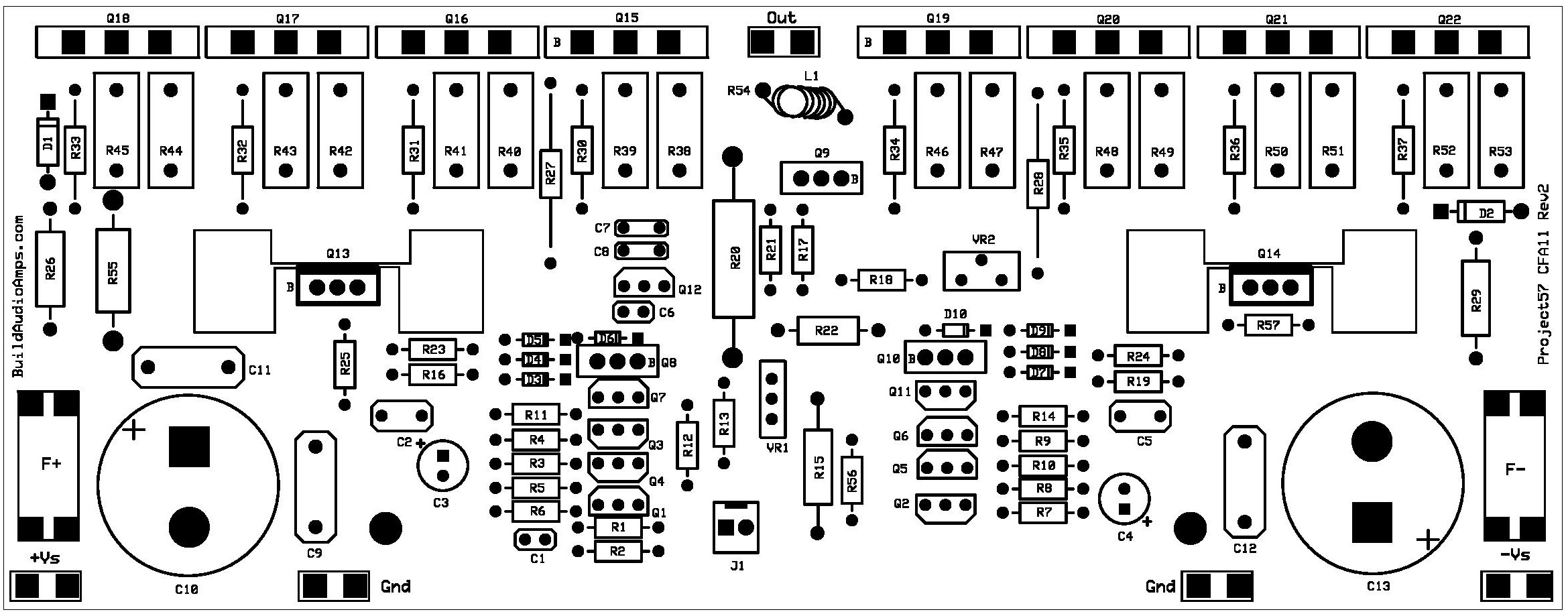
Project 57 Silkscreen, pads, text on top layer of PCB.
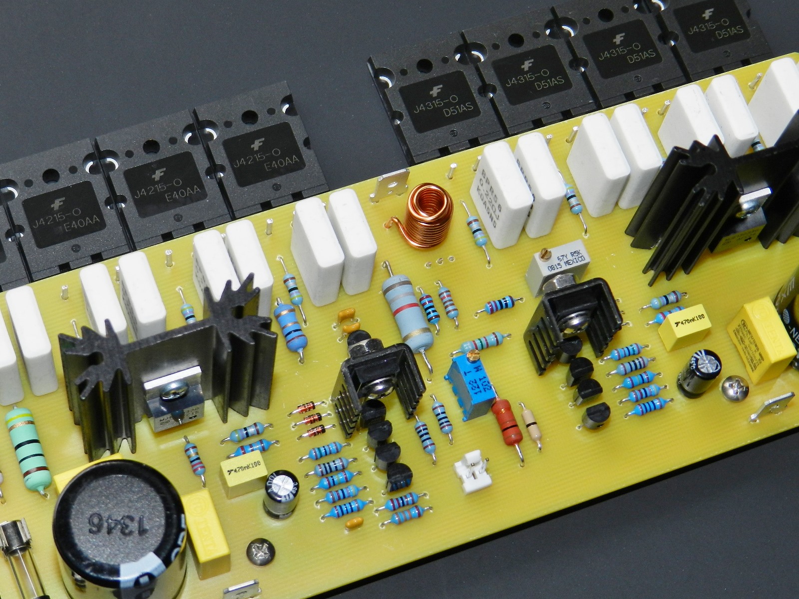
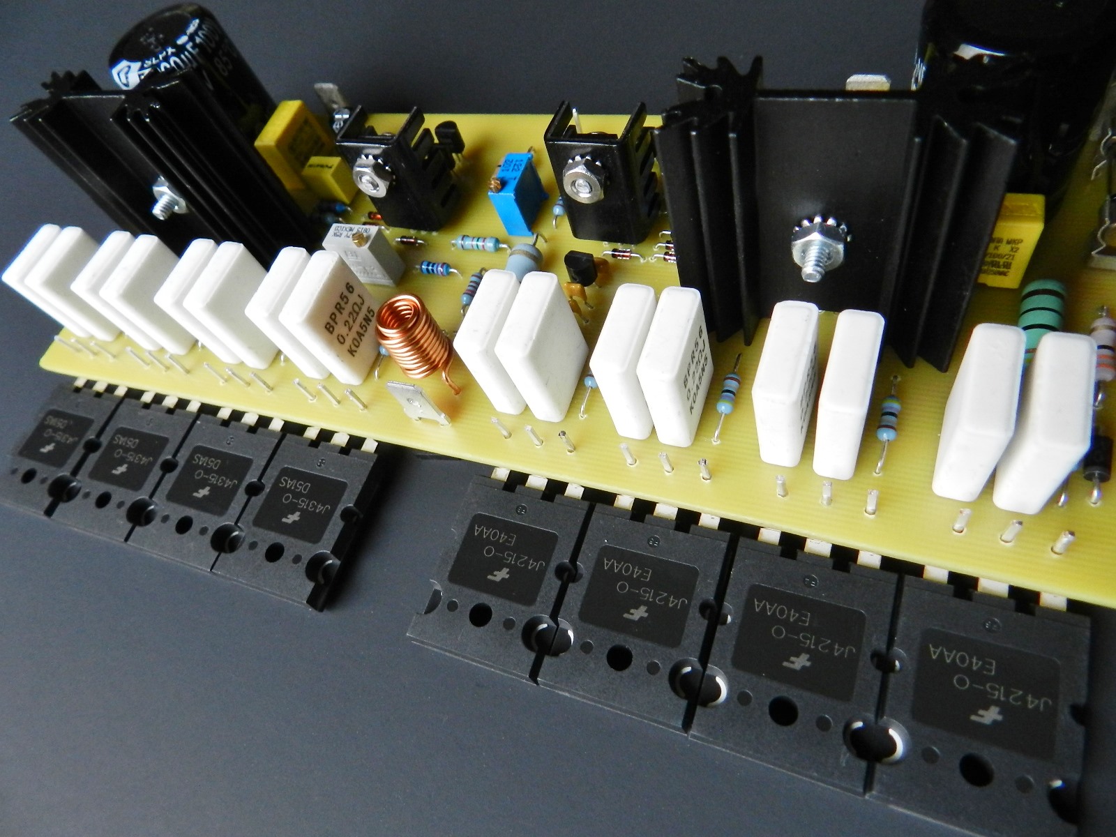
The prototype’s printed circuit board was created using ExpressPCB software, laser printed and etched to a 7.75” X 3” single sided copper board. The completed PCA is shown in the header pictures, while the completed prototype module is shown in the bottom pictures for reference. Transistor Q9, part of the bias circuit, is populated and soldered at the bottom copper side of the PCB. The TO-126-packaged transistor is generously applied with Wakefield PN 120-8 thermal compound or similar. The thermal compound fills up the small air gap between the transistor and the module’s aluminum mounting plate. Populated extensively in the output circuit are wirewound 5W radial power resistors, R38 through R53. These are connected at the collectors and emitters of all the power output transistors for stability and protection from thermal runaway. But the real kicker of this project is this ̶ the overall output of the amplifier is taken at the junction of all the collector resistors of the power transistors, Q15 through Q22. Capacitors C7 and C8 are some of the key components that determine the slew rate of the amplifier. The 25KHz and 100KHz square wave response of the amplifier are shown below.
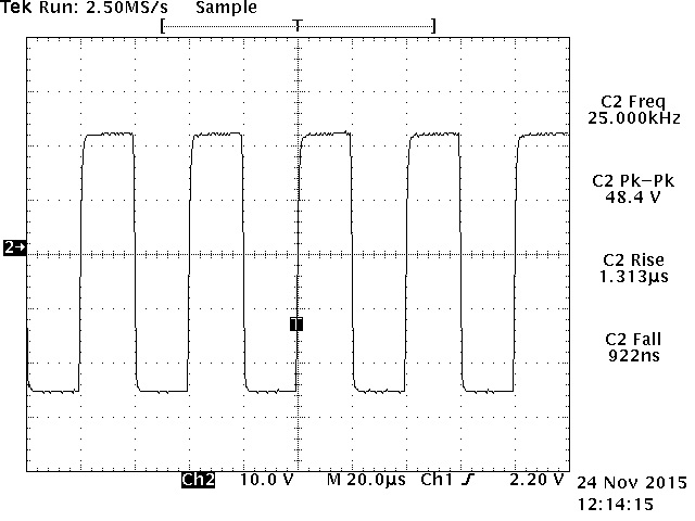

25KHz square wave response. 100KHz square wave response.

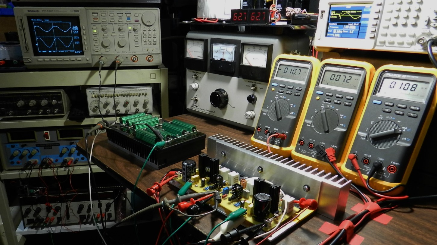
The picture shown above is the initial test setup and DMM readings of Project 57’s prototype. Also shown in the picture are two digital panel voltmeters that are permanently connected at the output of the test power supply and monitor the DC voltage rails. Before applying power to the amplifier, VR2 must be adjusted to minimum resistance (~0Ω). The test procedure was performed at an ambient temperature of 62°F. VR1 and VR2 were adjusted after a warm-up period of more than 30 minutes. Assuming an error-free PCB assembly, the following will explain in detail the project’s initial test setup as shown in the picture above.
The DMM on the left is connected to the output of the amplifier (white and green test clips); this measures the output DC offset voltage of the amplifier at 0.3mV, acquired by adjusting VR1. The DMM in the middle is connected across R53 (red and black test clips, can be seen on the right side of PCB); this measures the voltage drop across the emitter resistor of Q22 at 5.6mV. The voltage drop of 5.6mV divided by the resistance value of the emitter resistor at 0.22Ω is equal to the bias current of Q18/Q22 transistor pair at 25mA. The same 5.6mV reading should be approximately present across R47, R49 and R51. The DMM on the right is connected at the F+ fuse terminals (red and black test clips as seen on the left side of the PCB); this measures the total current drawn by the amplifier at about 99mA and is dependent on the adjustment of VR2.
Proceed to listening test if you have obtained the same DMM readings, as explained in the preceding test procedure, otherwise you may perform the next optional power output, square wave response and QA400 tests.
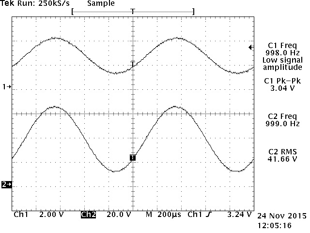
The picture above on the left shows the test setup for power output and square wave response test. The power output measurement requires a signal or function generator, oscilloscope and high wattage 8Ω dummy load. The signal generator is connected at the input of the amplifier (J1) that is set to about 1KHz sinewave output with its amplitude adjusted from 0 to about 3.04Vpp. This is the maximum input signal before clipping occurs at the output. The 8Ω dummy load is connected across the output of the amplifier under test. The CH1 probe of the oscilloscope is connected at the input of the amplifier, while the CH2 probe is connected across the 8Ω dummy load. The prototype produces about 41.66Vrms across the 8Ω dummy load; this corresponds to a power output of about 216.95 watts. A captured Tek hardcopy of the power output test result is shown on the right side picture above. R55 must be disconnected from the output circuit during square wave response tests to avoid damaging this resistor. The 25KHz and 100KHz square wave response test results were shown earlier.
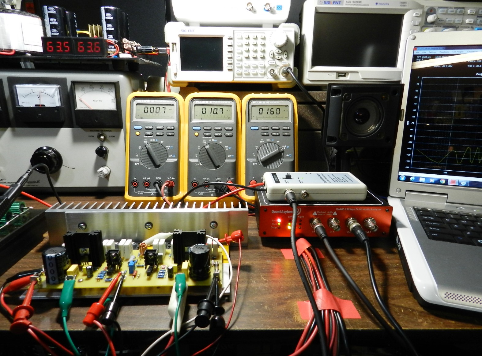
The picture above shows an 8Ω dummy load, Project 57, QA190, QA400, DMMs, Variac/power supply and a laptop computer. This is a simple test setup in performing basic audio measurements to Project 57’s prototype with very good results. A QA400 24-bit Real Time Audio Analyzer from QuantAsylum was utilized to measure noise, THD, THD+N, SNR and frequency response. The QA400 is USB powered, controlled by its own application software and can generate and analyze very accurately a series of burst test tones. For this test, the USB hardware was connected to a battery-powered laptop computer that’s running a Windows 7 operating system.
The input clipping level on the QA400 is +3dBV or 4Vpp. As it is, that’s good enough for testing low-voltage level preamplifier or tone control projects. It is however a problem when testing a power amplifier that’s producing very large amount of output voltage. To avoid this damaging condition to the QA400, it is necessary to attenuate the high voltage signal coming from the output of the power amplifier project. One of several ways is to connect a QA190 Low Noise Differential Probe to the input of the QA400. The QA190 clamps the high-voltage signal to safe level of about ±4 volts. The QA190 is battery powered and is also fitted with a selectable /10 and /100 range switch for convenience.
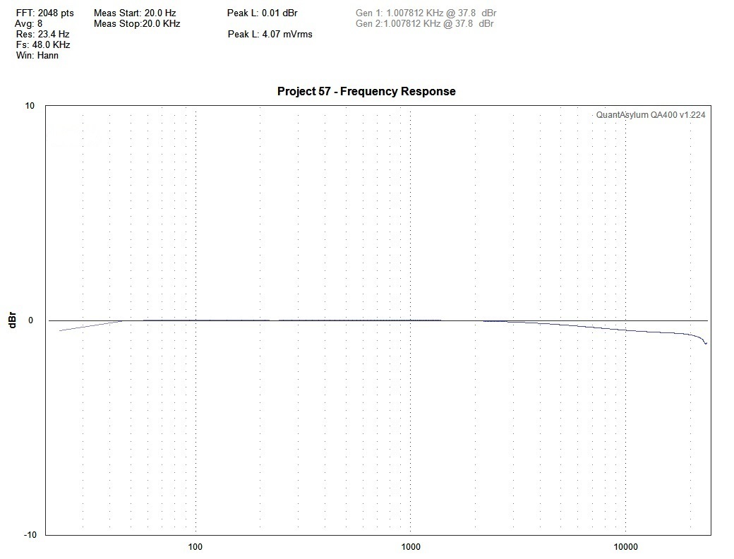
The left or right channel signal generator output of the QA400 is directly connected to the input of the amplifier under test. Depending on the type of measurement, the signal generator generally generates a 1KHz sine wave signal at -10dB with a sweep span from a start frequency of 20Hz to a stop frequency of 20KHz; however, all these values are user definable.
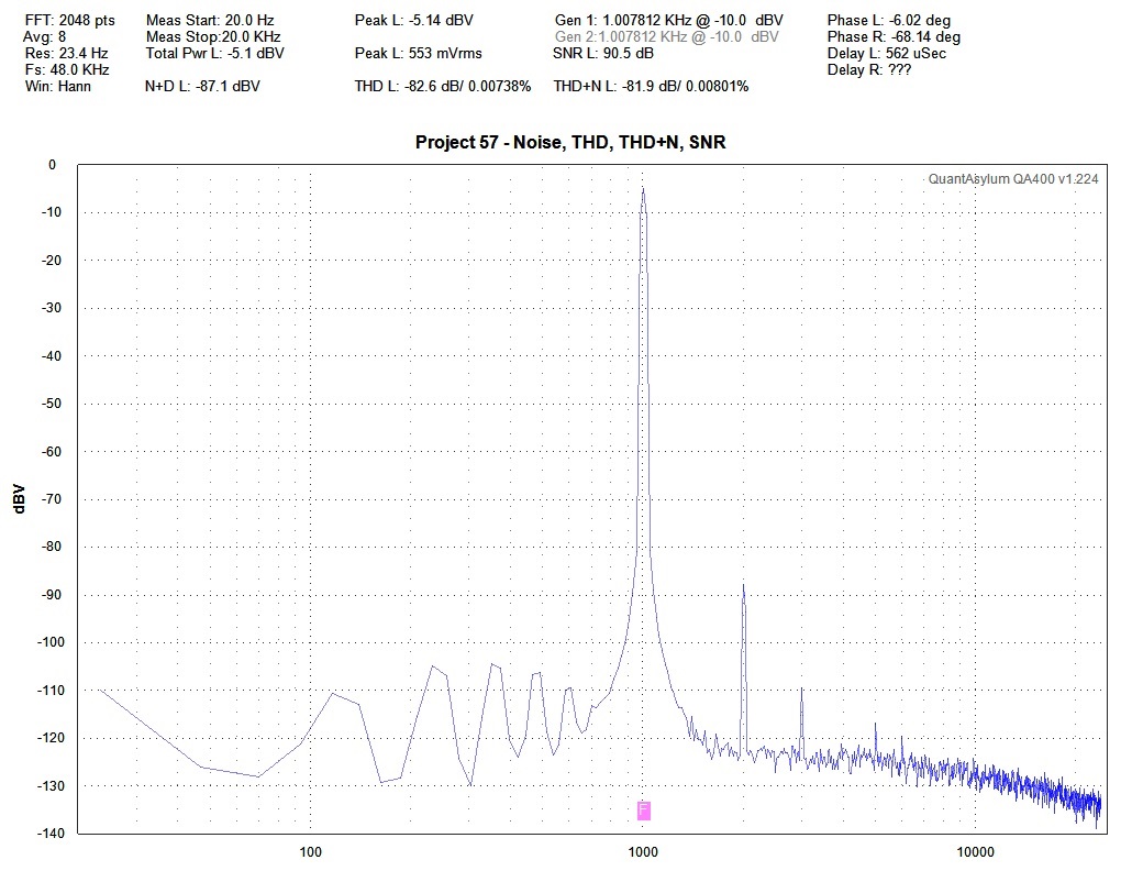
The next captured QA400 display area pictures will show the test results of Project 57.
How does Project 57 sonically perform in listening test? The prototype unit was connected to a passively modified LM49720 tone control preamp, a Toshiba HD-A2 player and several test speakers that are paralleled to produce an impedance from 3Ω to 4Ω. With various CD albums, the listening experience was extraordinary and did not disappoint, considering that this is a combination of CFA and CFP based audio power amplifier. The amplifier reproduces very clean impressive audio quality.
Previously, Phillips launched the professional “Golden Ears Challenge” training program. This is a test of how good your ears are able to detect slight differences in sound quality based on timbre, details, spatial impression, bass and loudness attributes. I took the challenge, completed and was awarded an elite Expert Listener by Philips.