Project 54

Project 54 is another CFA-based audio power amplifier project with a quasi-complementary power output stage topology. The measured power output is about 306 watts into an 8Ω load with ±80VDC power supply rails.
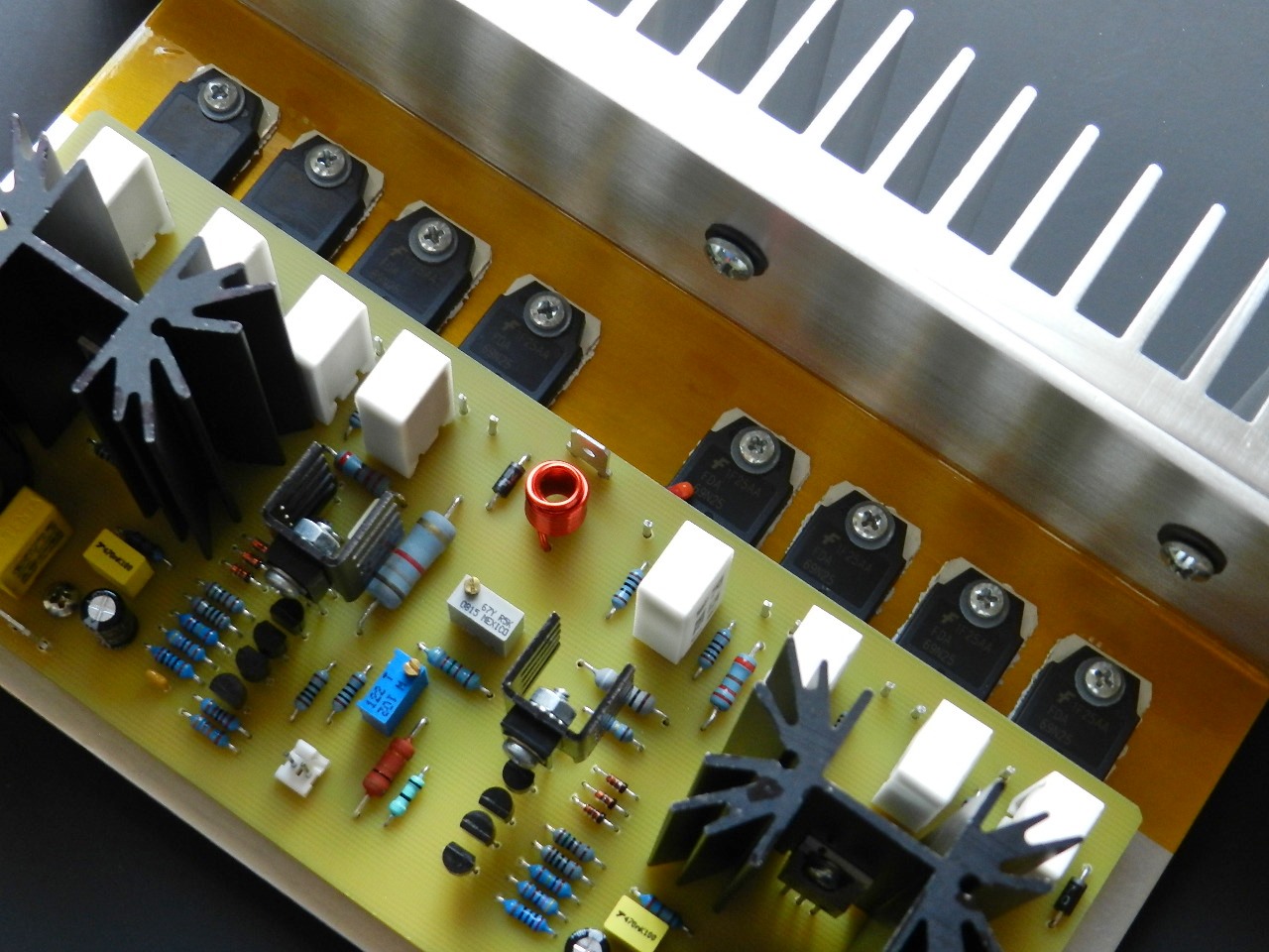
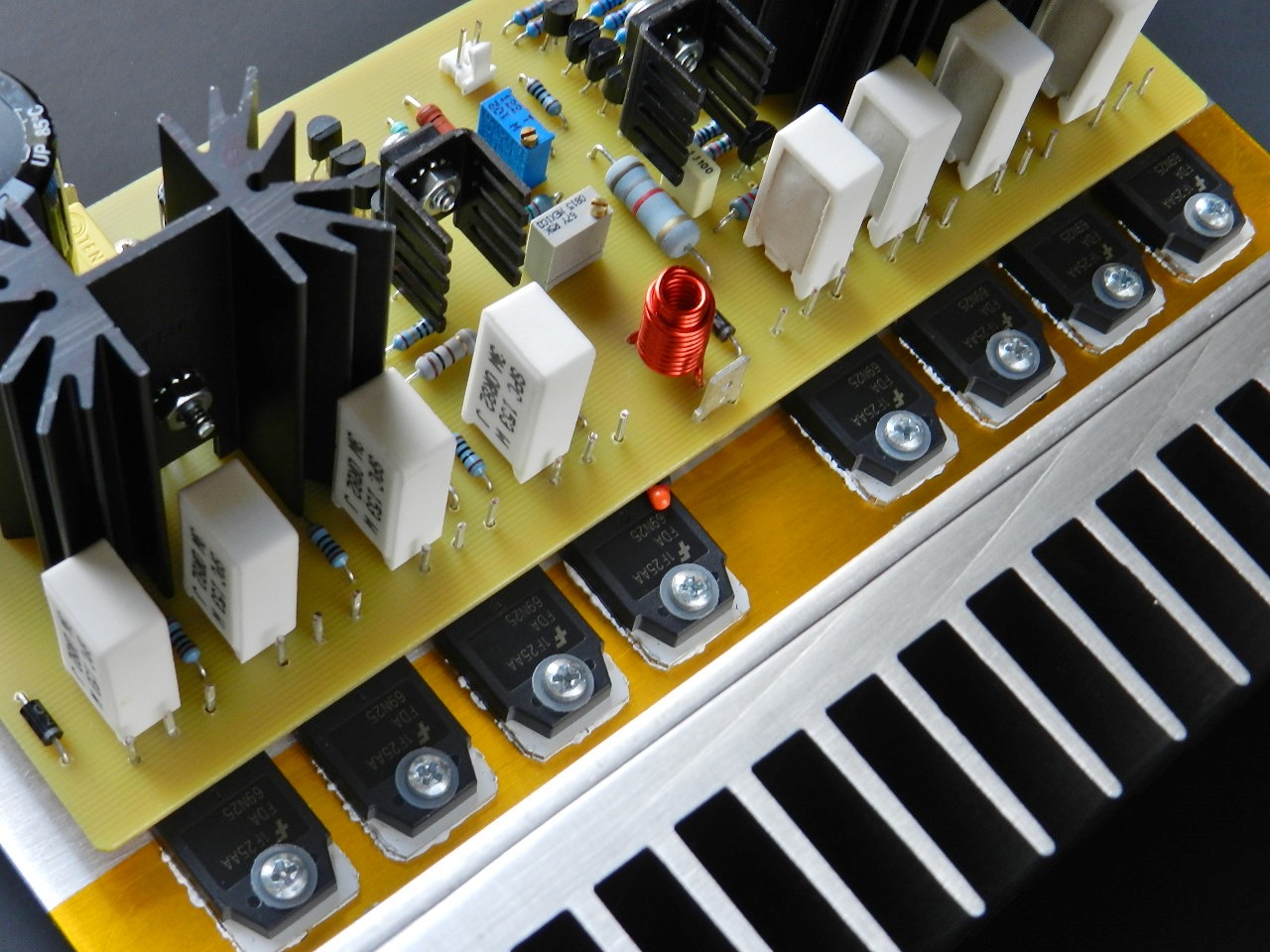
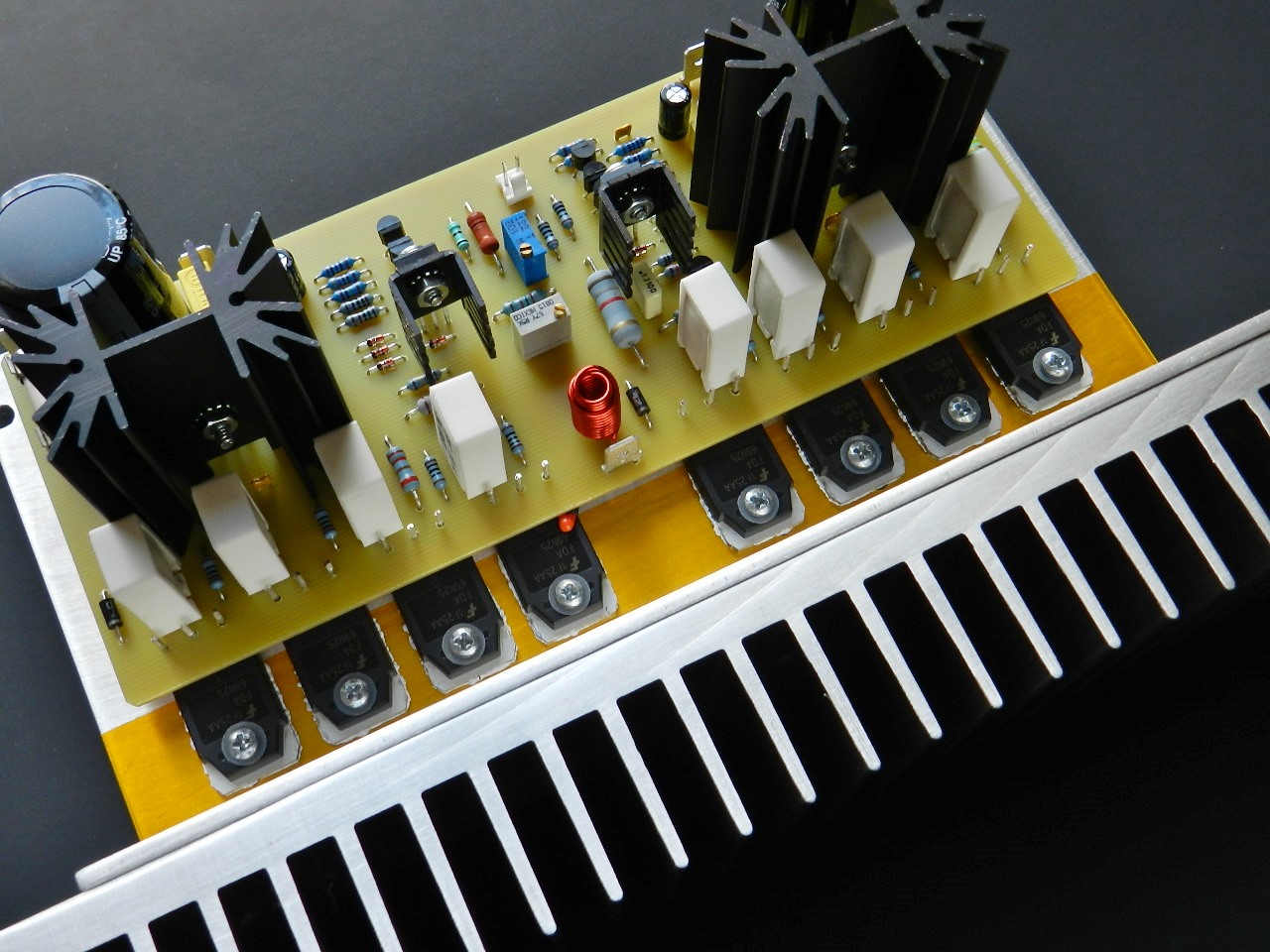
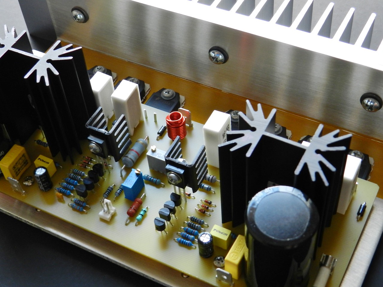
The project features all N-channel UniFET MOSFETs from Fairchild Semiconductor. Consequently, there’s no problem of searching for an appropriate matching complementary pair. Although the power MOSFET was designed for use in switching power converter applications, it is however utilized in this project and performed satisfactorily in all tests. The TO-3PN device is rated at drain-source voltage of 250 volts, drain current of 69 amps, power dissipation of 480 watts and drain-source on-resistance of 34 mΩ.
The implemented input stage of Project 54 is similar to those used by previous CFA-based audio power amplifier projects. The CFA-based input stage, in my opinion, produces better audio performance and quality when compared to the front-end input stage of a mirror-image topology presented in Project 44.
A feature of this project is the addition of an NTC thermistor in the VBE multiplier circuit. This technique offers better thermal stability when compared to other typical methods. A thermistor is a temperature-sensitive resistor that allows large changes in resistance in proportion to small changes in temperature. This resistance change cause by the rise in temperature effectively adjusts the base voltage of Q9, and as a result the bias of the output stage power transistors changes. In the prototype this thermistor is populated off the PCB as shown here. In previous projects it was the role of the VBE transistor to sense the rising temperature and control the bias of the power output stage transistors. It was also populated off the PCB and mounted in close proximity to the output power transistors.
The power output stage driver transistors, Q12 and Q13, are complementary pair arranged as emitter-follower and common-emitter configuration. Q12 drives the positive half amplifying output devices while Q13 for the negative half amplifying output devices. If these were to drive a complementary pair of power output transistors, as in a double or triple, both drivers would certainly be arranged as emitter-follower configuration. However, in this project these are driving the same type of output power transistors (quasi-complementary) therefore Q13’s output must be taken at the collector circuit. Q13 provides the required phase inversion of the pre-amplified signal needed by the paralleled output power transistors, Q18 through Q21. The emitter-follower driver transistor, Q12, provides the non-inverted pre-amplified signal needed by the paralleled output power transistors, Q14 through Q17.
A frequency compensating capacitor, C14, is populated and soldered on the copper side of the PCB, as an afterthought! In listening test without this capacitor the high frequency response was overly exaggerated – this contains undesirable overshoots in square wave response tests. This capacitor is one of the components that determine the slew rate of the amplifier. Its capacitance value was chosen for optimum square wave response, that is, maximum rise time and minimum overshoot.
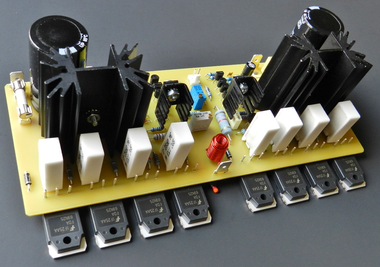
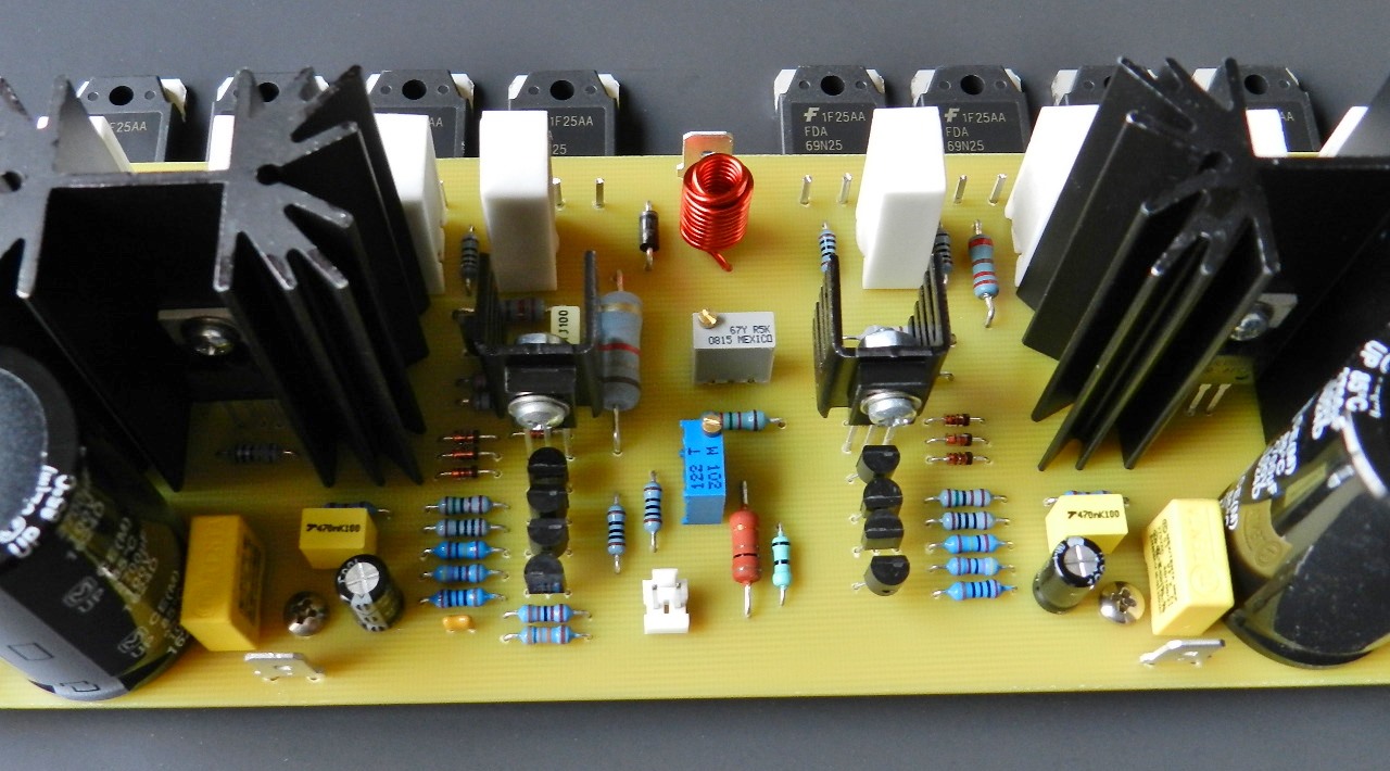
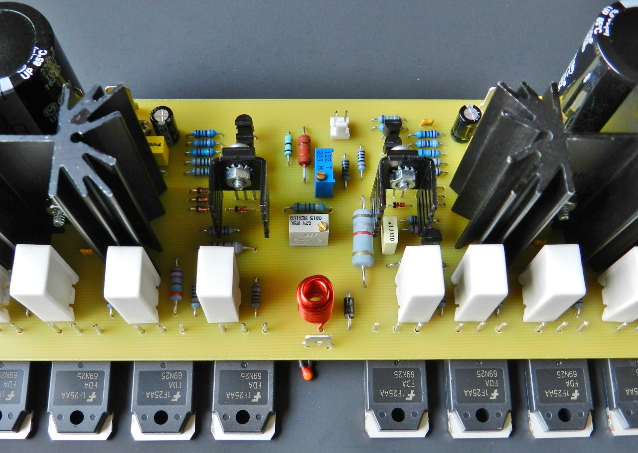
The prototype model was built on a 7.75” X 3.0” single-sided PCB. All components used in the prototype model are readily available standard parts. PCB assembly is fairly straightforward. The populated PCB assembly is shown in the header pictures while the completed prototype module is shown at the bottom of this page. If you are interested in building this project and have read the Information and Policies section of this website, the schematic diagram, PCB layout and BOM (available only by request) are free, as is, no warranty.
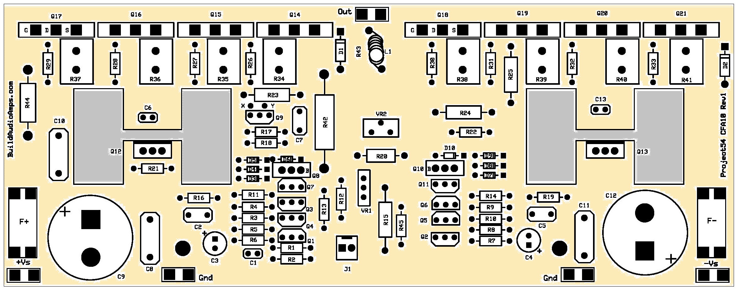 Project 54 Silkscreen parts placement layer of PCB.
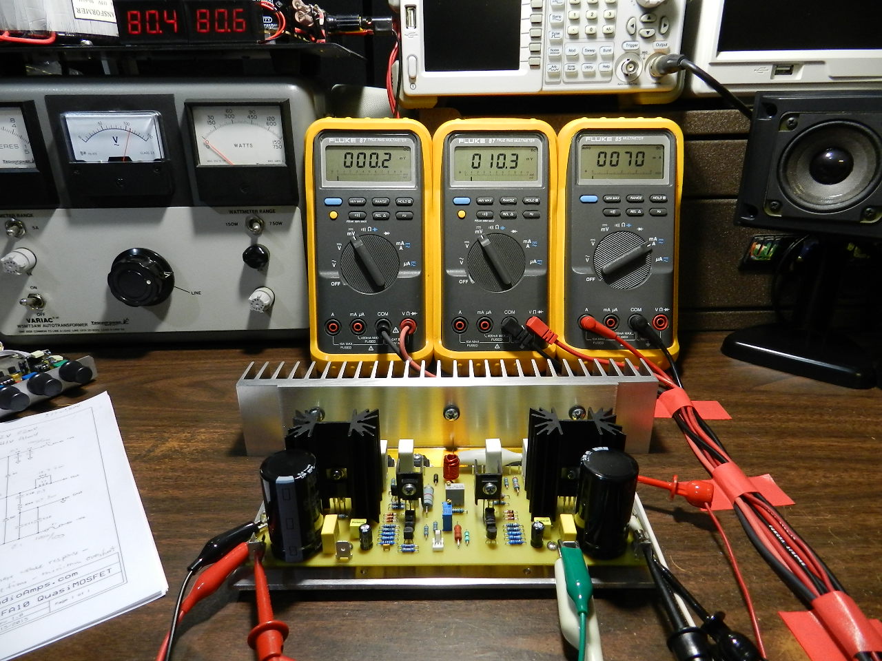
The picture above shows the initial test setup for adjusting VR1 and VR2. VR1 controls the DC offset voltage of the amplifier while VR2 controls the bias of the output stage power transistors. For testing purposes, the 2-wire digital panel voltmeters connected at the output of the power supply monitors the output voltages at +80.4V and –80.6V respectively. The power supply was connected to an overcurrent-protected Variac autotransformer. For this project, an AnTek AN-8455 or Avel Y236904 toroidal power transformer is recommended, rated 110VCT at 800VA.
Initially, with the power off, adjust VR2 to approximately 590Ω to 600Ω. Assuming an error-free PCB assembly, at power ON the idle current of the power transistors is about 155mA to 195mA per pair; this corresponds to a voltage drop across any source resistors, R38-R41, at 127mV to 160mV respectively. Don’t panic, this will eventually decrease because of TH1. After 15 minutes or so adjust VR2 from 10mV to 20mV depending on the builder.
The DMM on the left is reading the DC offset voltage at 0.2mV. The DMM in the middle is reading the voltage drop of any source resistors, R38 through R41, in this case R41 at 10.3mV. The DMM on the right is connected across the F+ fuse terminals and measures the overall current drawn by the amplifier at 70mA. These test results were acquired after a 15-minute warm-up period. With an ambient temperature at 27°C, the temperatures of the high-current transistors were measured. The pre-driver transistors, driver transistors and output power transistors’ temperature are at approximately 40°C.

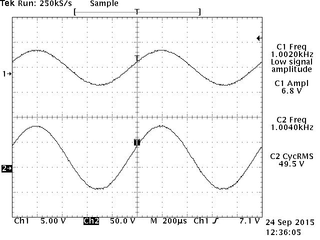
The picture above on the left shows the test setup for power output measurement and square wave response tests. Be careful not to touch the heatsink or dummy load when performing this test. After several minutes of testing with the input signal adjusted just before the clipping point of the output, the power transistors’ temperature rises to more than 80°C.
A signal generator was set for a sine wave output signal with its amplitude adjusted before clipping point at 6.8Vpp. The signal generator’s output was directly connected to J1, as well as CH1 probe of the oscilloscope. The 8Ω dummy load and CH2 probe of the oscilloscope were connected at the output of the amplifier under test. The picture above on the right shows the Tek hardcopy picture of the power output test result. The prototype produces 49.5Vrms across the 8Ω dummy load or 306.28 watts. When performing square wave response tests, R44 must be removed from the output circuit. Running a continuous high frequency square wave signal will damage this resistor. The 25KHz and 100KHz square wave response of the prototype shown below is made possible by C14.
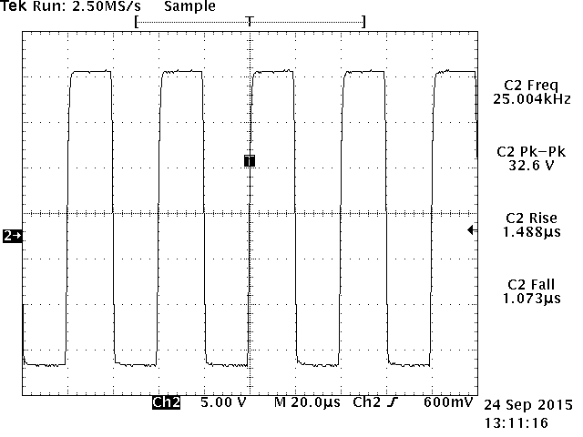
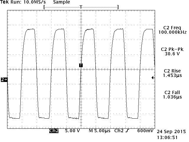
25KHz square wave response. 100KHz square wave response.
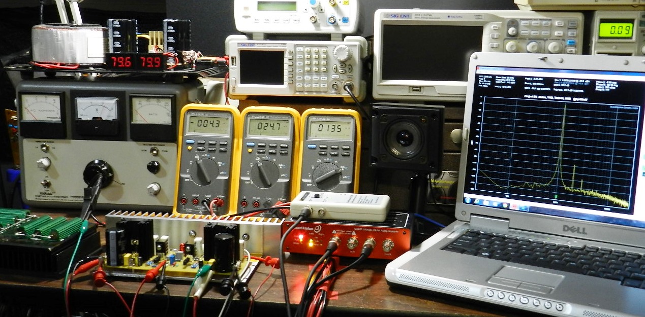
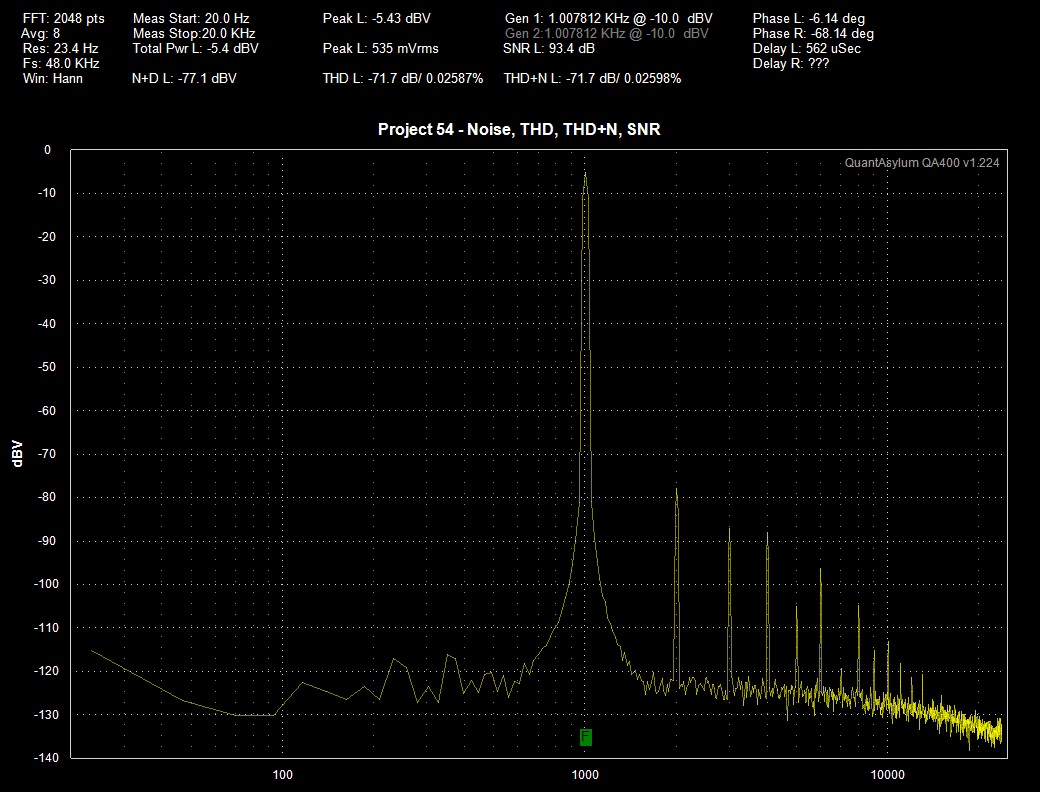
The picture above shows the Noise, THD, THD+N, SNR and Frequency Response test setup utilizing QuantAsylum’s QA400 USB-based 24-bit real time stereo audio analyzer and QA190 low-noise differential probe. The picture below shows the captured data test results.

How does it perform in listening test? The prototype unit was connected to a modified LM49720 tone control preamp, Toshiba HD-A2 player and a Kenwood MV-9D monitor speaker. Listening to several CDs, the audio quality is not the greatest nor unpleasant, it’s just satisfactory with well-defined powerful bass, in spite of the quasi-complementary topology and the absence of a Baxandall diode. Increasing the input signal level to higher than normal, this is where it gets its superiority!