Project 61
Project 61 is based on two well-known audio power amplifier designs, the Blameless Amplifier by Douglas Self and the Audiophile Amplifier by G. Randy Slone. Both designs have identical differential input and voltage amplifier stages and emphasize heavily in reducing distortions to their lowest possible level. The claimed THD figure comes close in comparison to the LME498xx specifications. Sadly, currently the LME498xx series of high fidelity power amplifier input stage from TI has an end-of-life product status. Nevertheless, by using both designers’ techniques the diminishing THD figure is likely achievable. Details of the circuit description of each amplifier design can be found in Douglas Self’s the “Audio Power Amplifier Design Handbook” as well as G. Randy Slone’s the “High-Power Audio Amplifier Construction Manual”. These are highly recommended reference resource books if you are into building or tinkering with high performance audio power amplifiers.
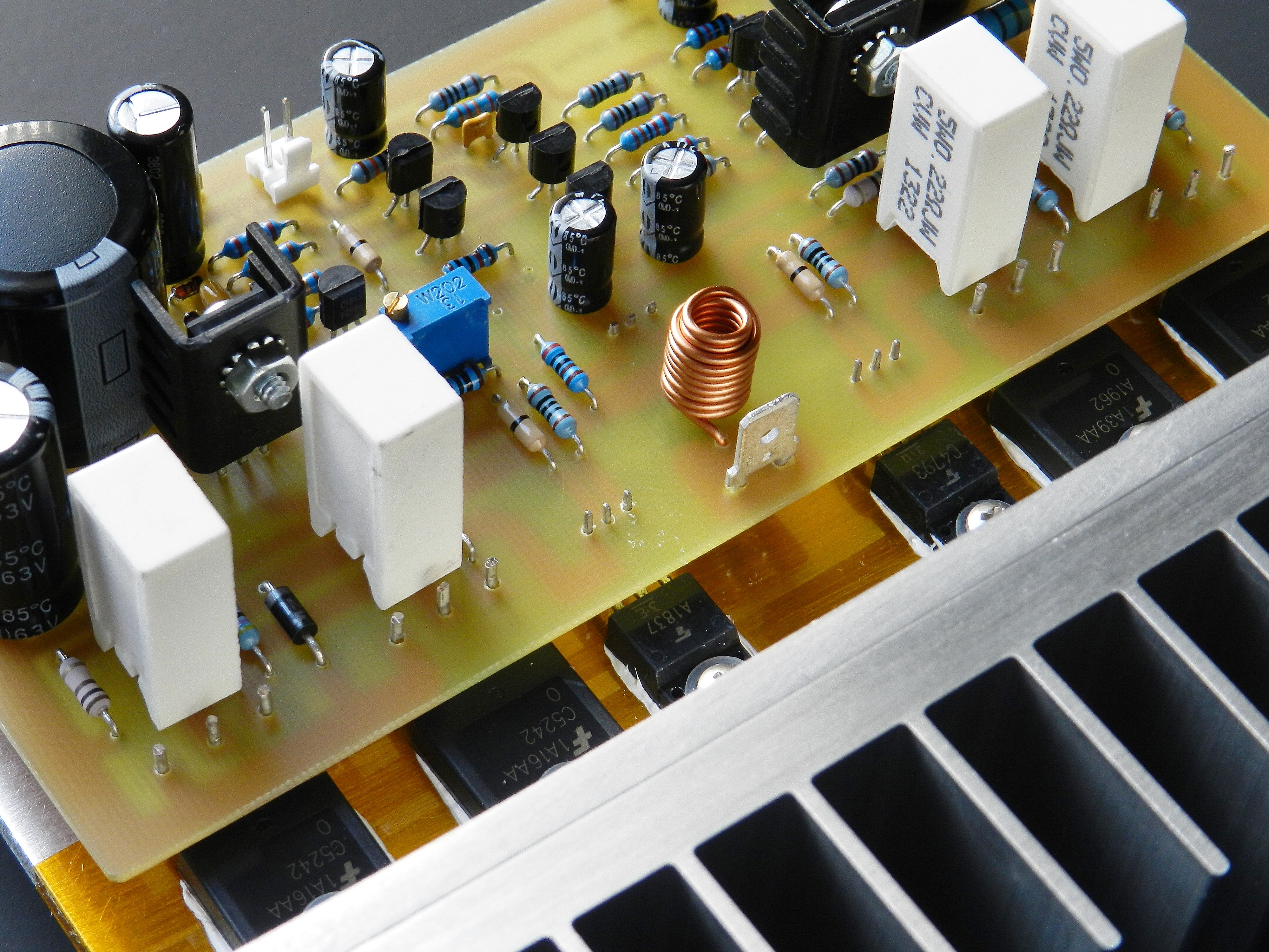
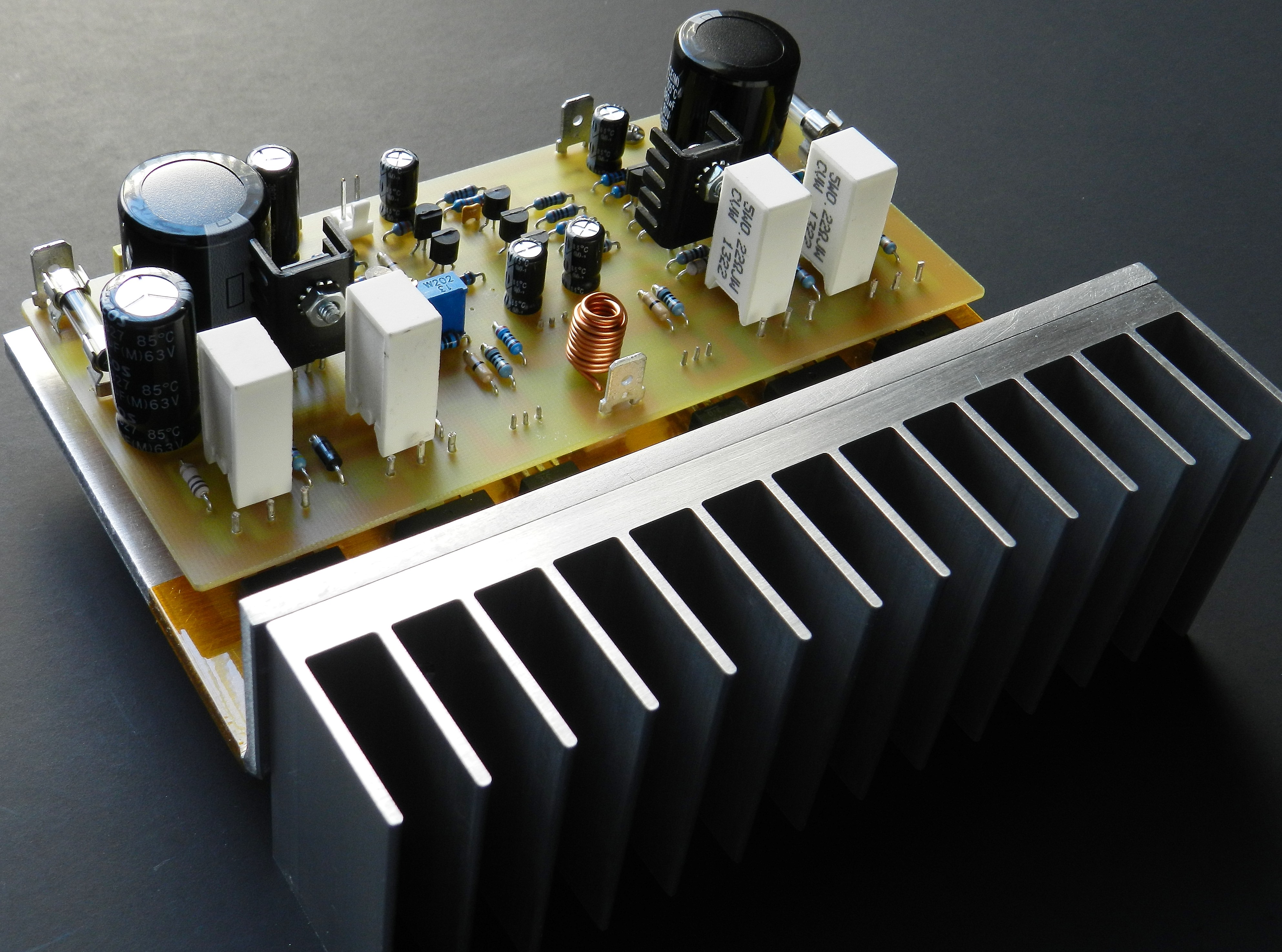
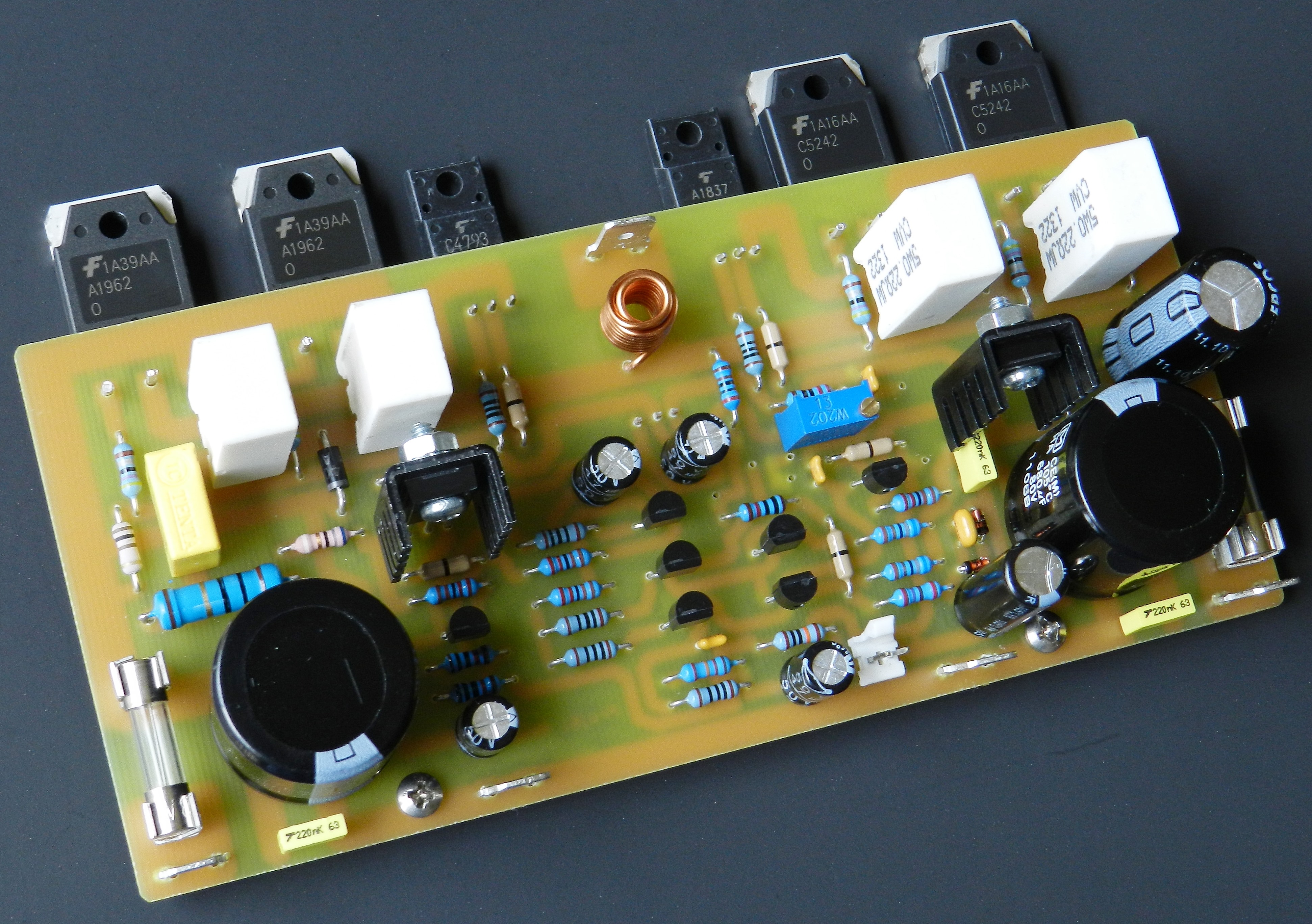
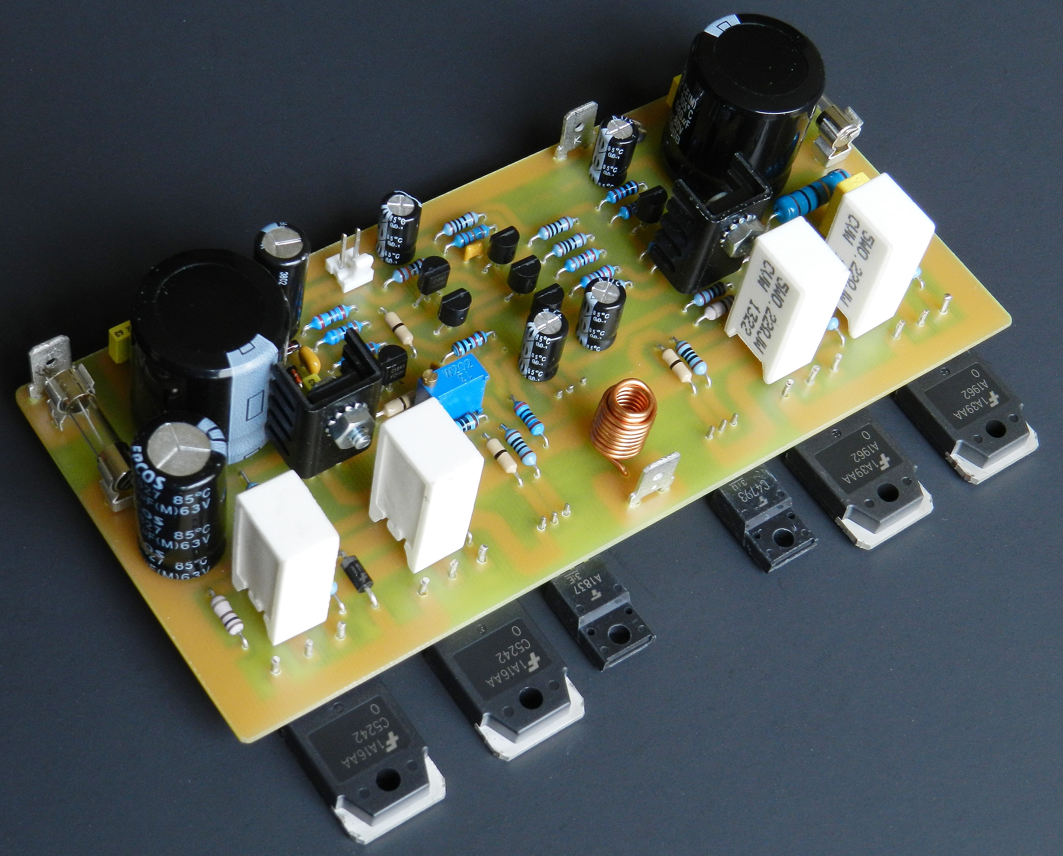
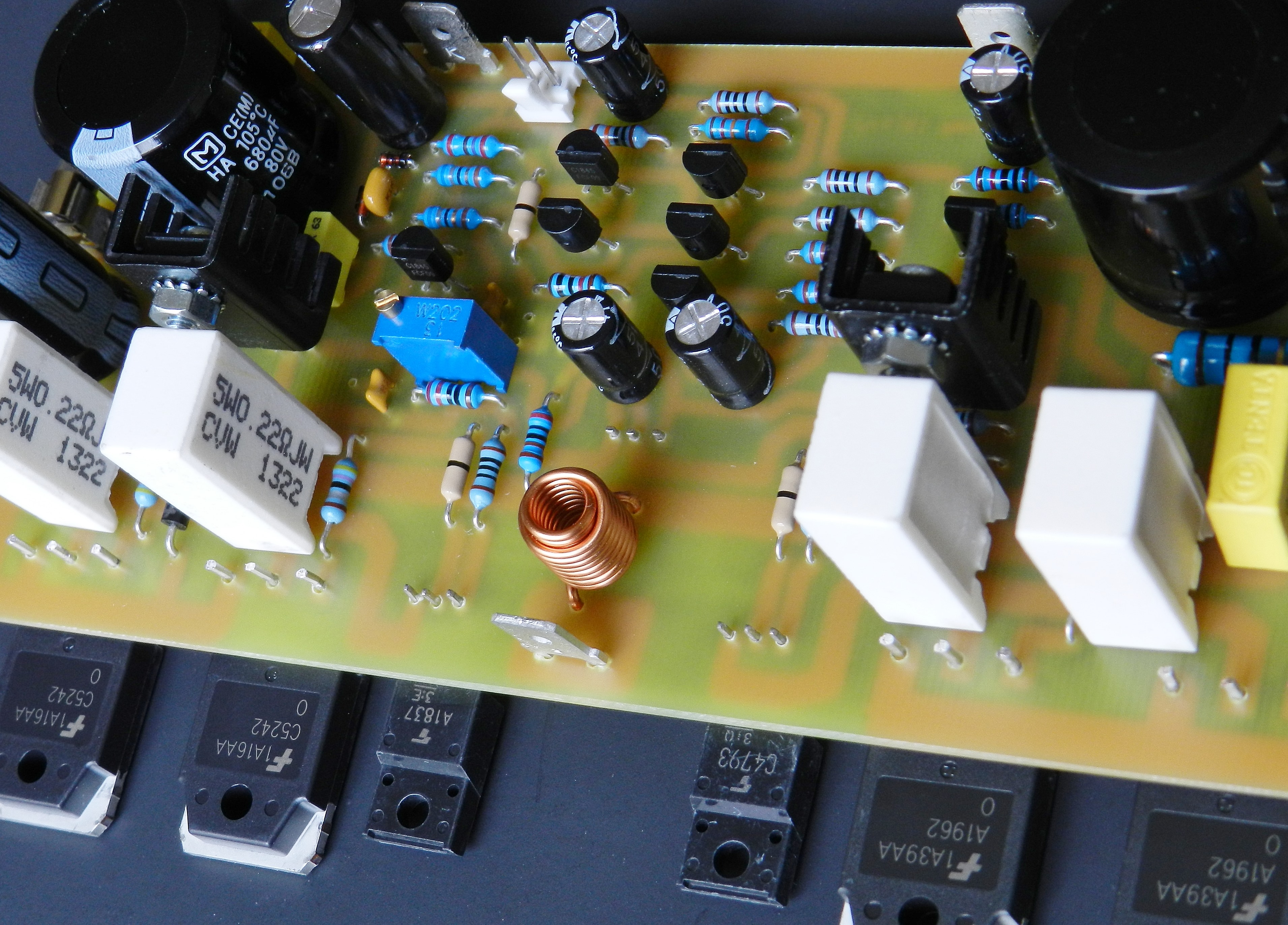
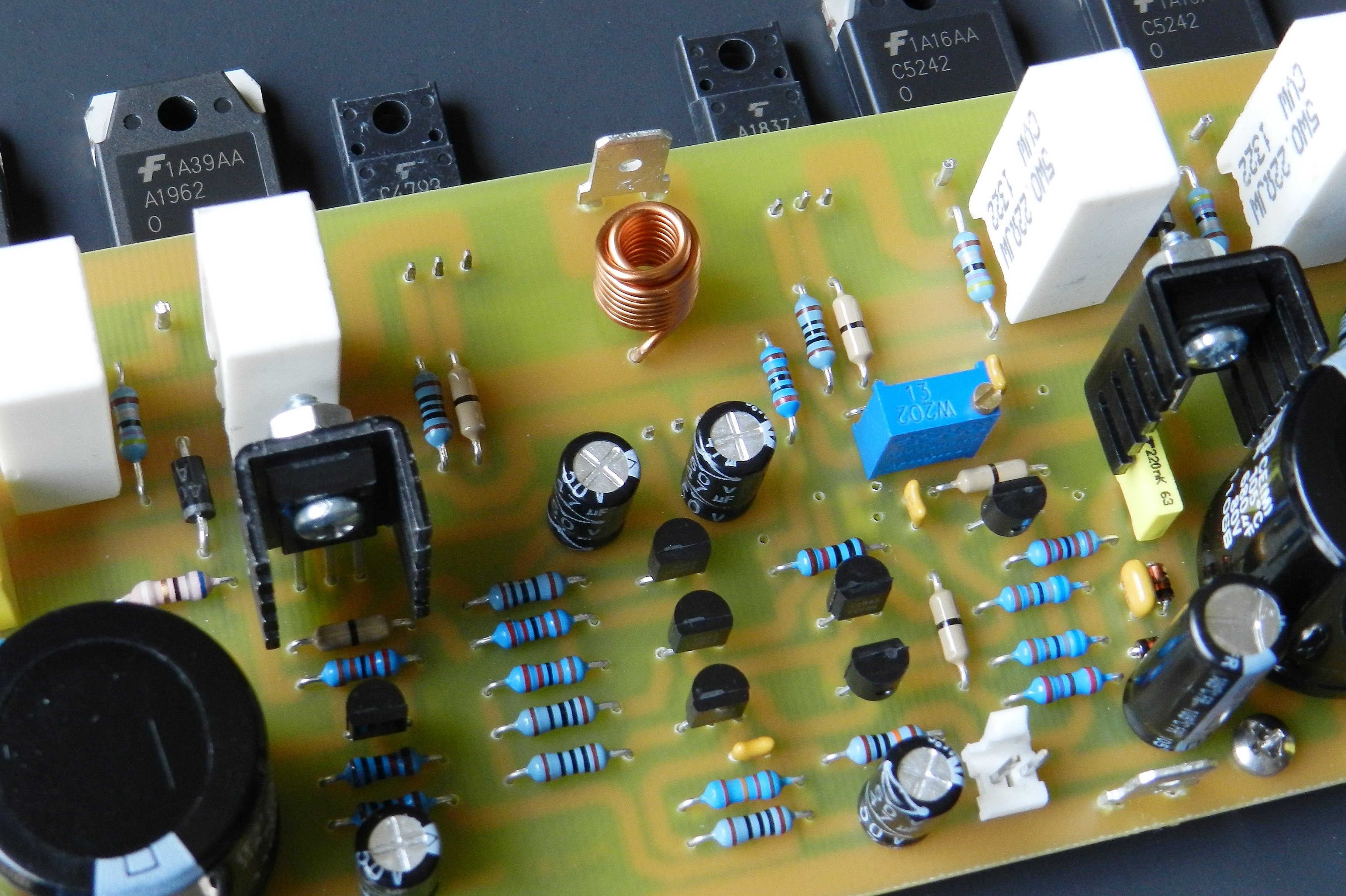
Because there are some circuit similarities between the two designs, it makes sense to come up with a combined schematic diagram for this project and this will be referred to from hereon. Project 61’s schematic diagram is found here and the BOM is found here. The prototype was created using ExpressPCB, laser-printed and etched into a single sided 6” X 2.725” PCB. Figure 1a shows the parts placement guide of a suggested PCB layout while Figure 1b shows a see-through top and bottom layer of the PCB for your convenience, if you are planning to make your own.
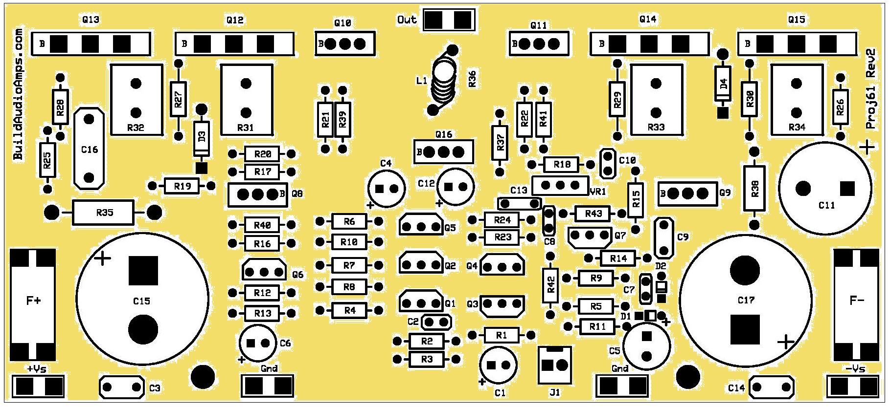
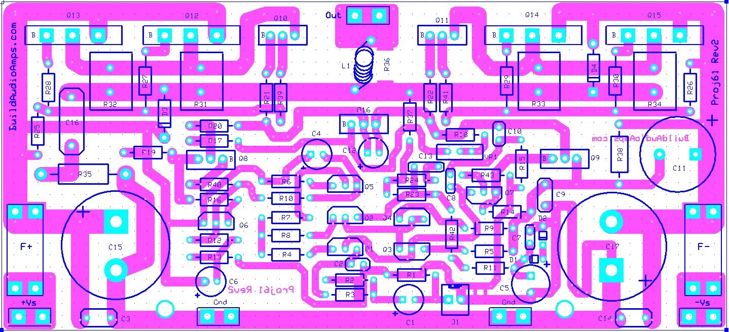
Figure 1a. Project 61 Silkscreen top layer of PCB. Figure 1b. Project 61 See-through top and bottom layer of PCB.
The preferred power output stage for this project is the paralleled complementary feedback pair (CFP) configuration. The measured power output of the prototype is about 110 watts into an 8Ω load with ±50VDC power supply rails. The ratio of R23+R37 and R11 determines the overall AC voltage gain of the amplifier. The measured input sensitivity of the amplifier to produce the full rated power output is approximately 0.5Vrms. Capacitor, C5, part of the negative feedback network, is made large enough so that it is audibly noticeable in the listening test. The current gain (hFE) of Q1 through Q7 is matched using a cheap DMM with built-in hFE range. This was suggested in the LeachAmp plan and in an article written by G. Randy Slone about his 200-watt audiophile amplifier. This proved to be an effective part of the build process to reduce the DC offset voltage of the amplifier to audiophile level.
The PCB layout has component placements for an RC network consisting of R24 and C13 in parallel with one of the main negative feedback resistors, R23. However, when included in the feedback loop this causes high frequency noise or spikes in the waveform during power output measurement. Increasing the value of R24 would somehow fix the problem, but this requires further experimentation. Consequently, R24 and C13 were unpopulated in the prototype with Figure 8 showing the conclusive test result. Generally, these components have specific function of reducing the bandwidth of the amplifier or it could define the amplifier’s tone character (why this amplifier sounds different from the others).
Again, the PCB layout has other component placements intended for a two-pole compensation network consisting of R15, C8 and C10 in the voltage amplifier stage. However, in square wave testing it produces ringing when R15 is 1KΩ and an overshoot when R15 is 6.8KΩ as shown in Figure 2 and Figure 3, respectively. The prototype had R15 removed, which makes the total series capacitance of C8 and C10 to approximately 68pF. This will also transform them into a typical single-pole compensation capacitor. The improved 25KHz and 100KHz square wave test results, with R15 removed, are shown in Figure 4 and Figure 5. Although populating the two-pole compensation network into the circuit is hardly noticeable during listening test, it’s up to the interested ampbuilder to decide its inclusion into their project.
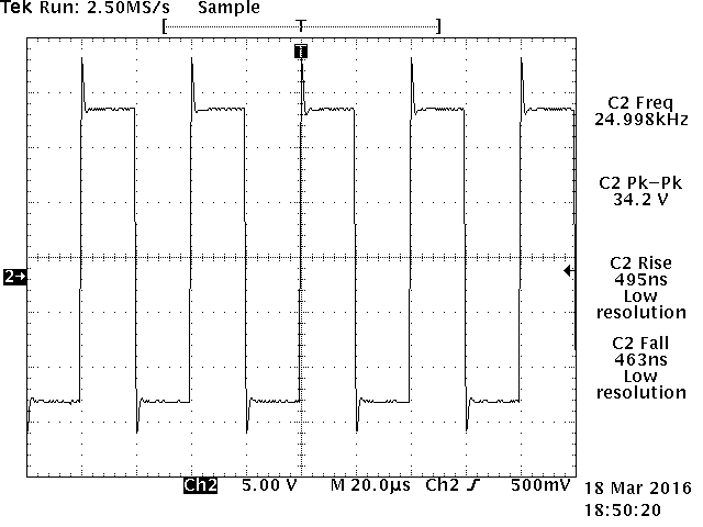
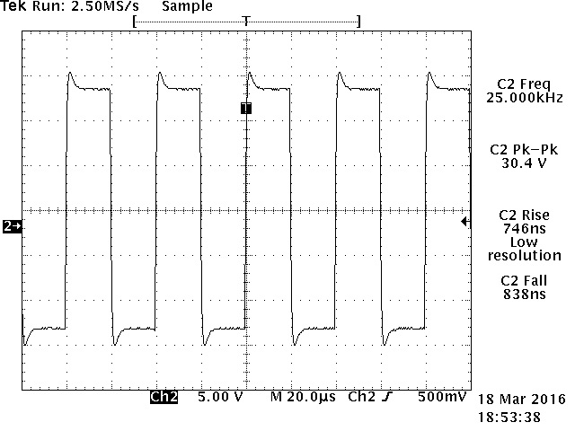
Figure 2. 25KHz square wave test result with HF ringing. Figure 3. 25KHz square wave test result with HF small overshoot.
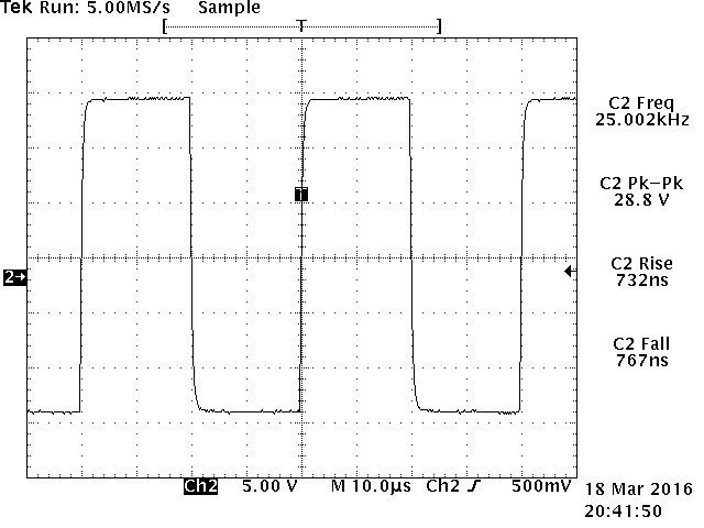

Figure 4. 25KHz square wave test result with R15 removed. Figure 5. 100KHz square wave test result with R15 removed.
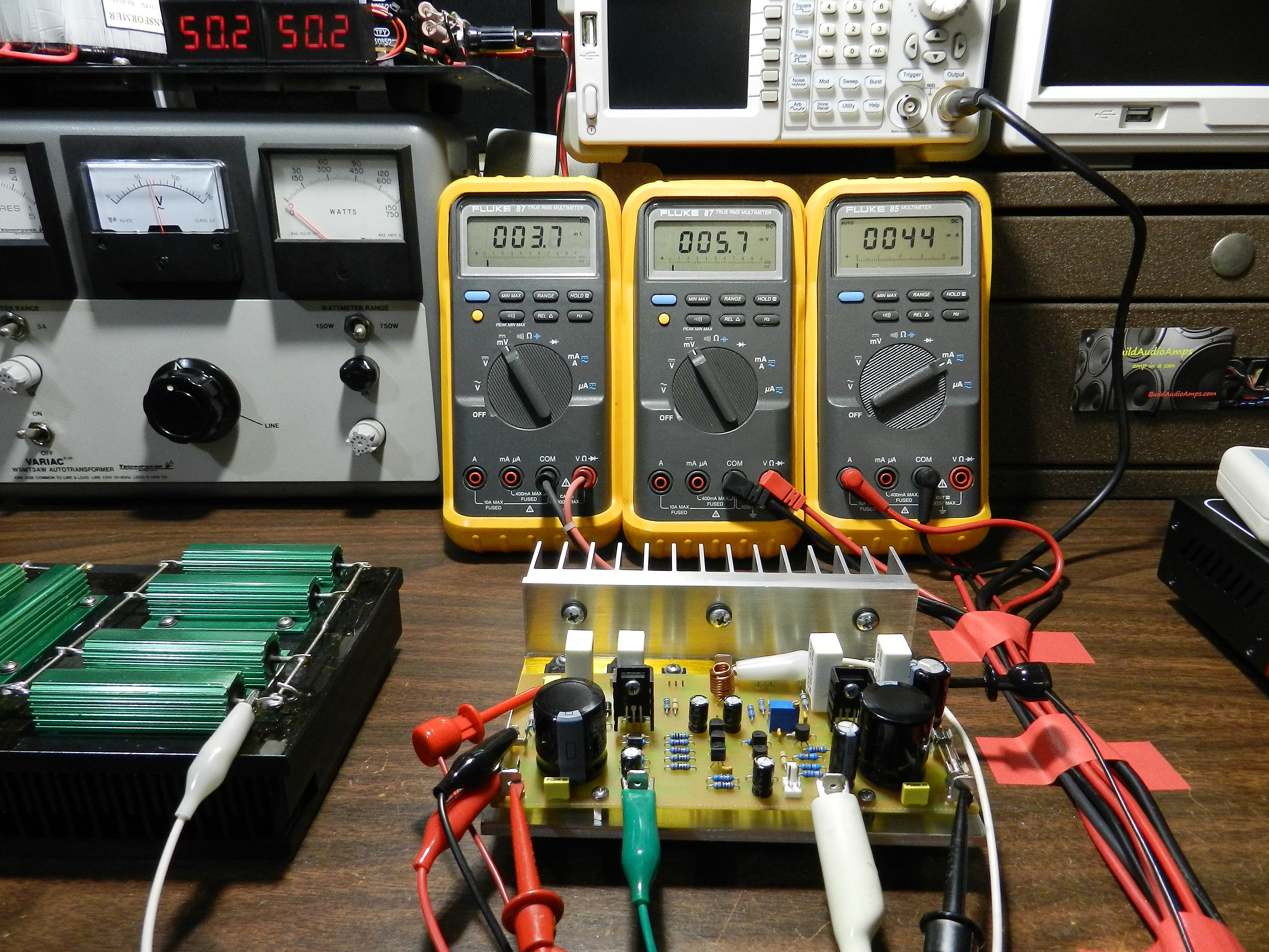
Figure 6. The initial test setup of Project 61.
You may proceed with whatever convenient method you are using in testing a newly built amplifier. As a rule, however, the output stage power transistor’s quiescent bias needs to be adjusted first to enable the amplifier project to operate properly. The initial test setup for this project is shown in Figure 6.
If a Variac autotransformer is available, set the voltage adjust knob to minimum setting before applying power to the unit. Adjust VR1 to its maximum resistance. The AC output voltage of the Variac is connected to the AC input voltage of the test power supply. The test power supply has two digital panel DC voltmeters that are connected to the positive and negative output voltage rails, as shown in Figure 6. This is a convenient way of constantly monitoring the status of the dual output voltage of the test power supply.
Apply power to the Variac and gradually adjust its output voltage so that the rail voltages of the test power supply are about ±50VDC while at the same time observing for any unusual DMM readings. Any higher DMM readings than the one shown in Figure 6, immediately switch the power to OFF and check for any wiring or PCB assembly errors before proceeding with the test procedure.
The DMM on the left of the picture is connected at the output of the amplifier, this measures the DC offset voltage. The DMM reads 3.7mV and this could be anywhere from near zero to about less than 10mV, mainly because of the hFE matching as earlier mentioned. The DMM in the middle is connected across the collectors of Q12, Q13 and collectors of Q14, Q15. This measures the voltage drop of all the collector power resistors at 5.7mV, which sets the total bias current applied to all power transistors at approximately 26mA. The voltage drop could be anywhere from 5mV to 15mV depending on the ampbuilder. The DMM on the right is connected across the F+ fuse terminals and measures the total current drawn by the amplifier at 44mA. This is dependent to the setting of VR1.
There is a “turn-on thump” through the loudspeakers when the amplifier is powered up. The amplifier produces an output voltage of a few millivolts in a mere fraction of a second that is applied to the load or the loudspeaker system. It’s not scary at all when some ampbuilders including myself uses a 3-volt or even a 9-volt battery to test the loudspeaker’s cone movement. Most good speakers, including the bench test speakers, will survive the “turn-on thump” indefinitely. However, a simple speaker protection circuit similar to the “uPC1237 Speaker Protection and Power ON Delay Project” may be implemented for peace of mind.
After performing the initial test procedure you may proceed with music listening test or continue with the next optional tests.
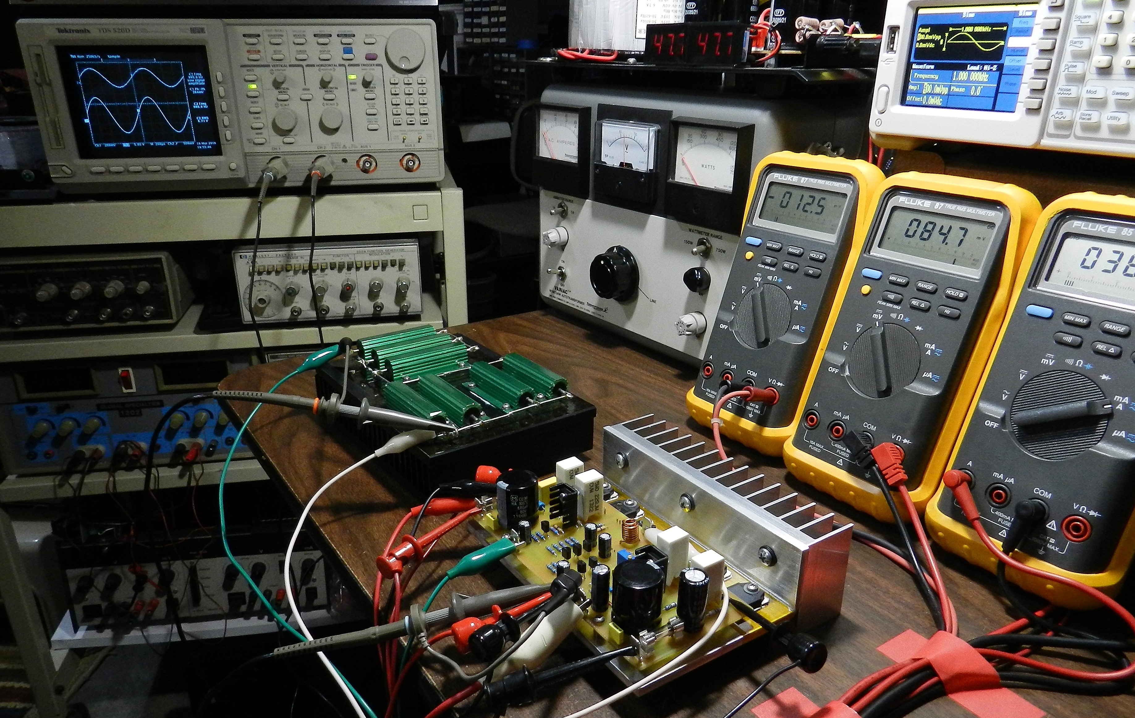
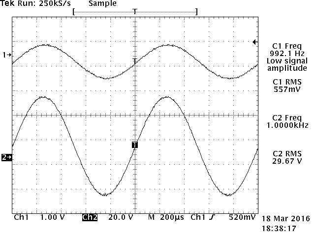
Figure 7. Power output and square wave test setup. Figure 8. Power output measurement test result.
Figure 7 shows the test setup for power output and square wave response measurements. Be careful not to touch the amplifier under test, heatsink or dummy load during this test because they will get very hot. An SDG805 function/arbitrary waveform generator and Tektronix TDS520D 500MHz oscilloscope were used for these particular tests or any similar equipment that you may already have. The dummy load is connected only during power output measurement. The 2-watt resistor, R35, should be disconnected from the amplifier during 100KHz square wave response test. Running a continuous high frequency square wave signal to the amplifier will burn-up this resistor.
The power output of the amplifier just before clipping is about 110watts at 8Ω with ±50VDC power supply rails. This power output was acquired by applying a 557mVrms of 1KHz sine wave input signal to the amplifier, which produces about 29.67Vrms across the 8Ω dummy load. The Tek hardcopy picture of the power output test result is shown in Figure 8. Shown earlier in Figures 4 and 5 are Tek hardcopy pictures of the 25KHz and 100KHz square wave’s rise and fall time measurement output waveforms.
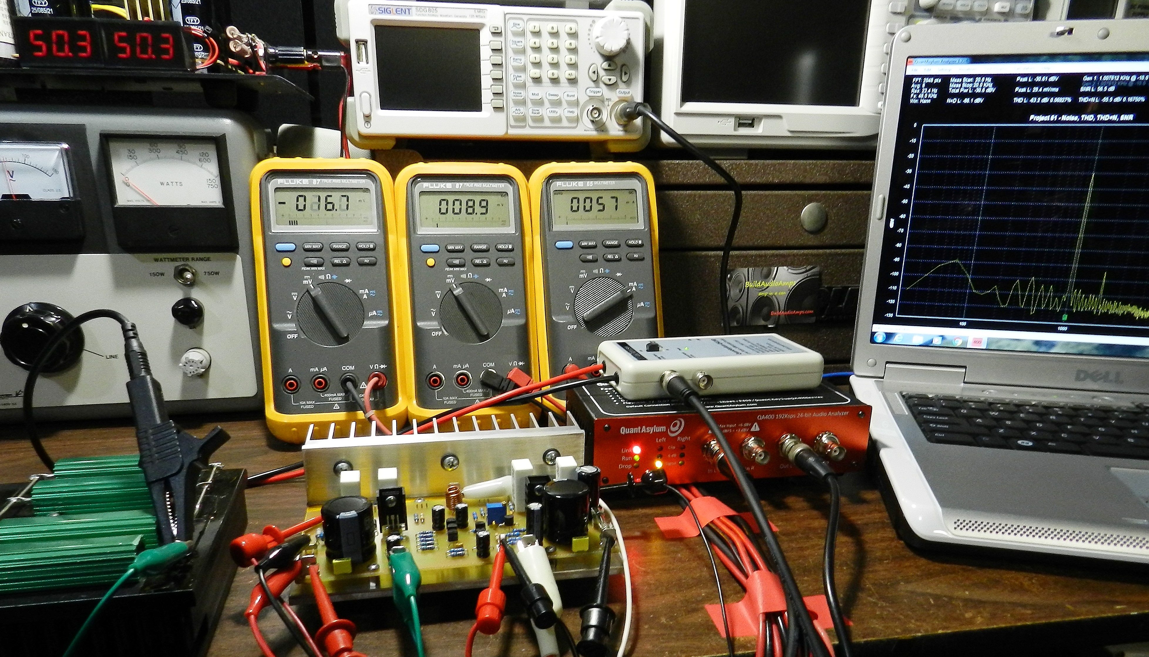
Figure 9. QuantAsylum’s QA400 and QA190 audio analyzer test setup.
Figure 9 shows the basic audio analyzer test setup - utilizing a QA400, QA190, an 8Ω dummy load and a laptop computer. This is a simple test setup in achieving several audio measurements and analysis to the power amplifier project with very good results. Figure 10 shows the Noise, THD, THD+N, SNR test result while Figure 11 shows the Frequency Response test result.
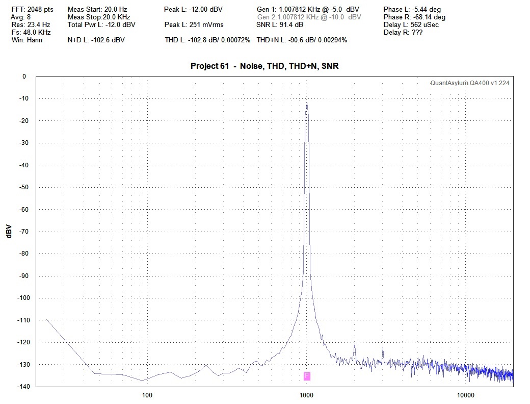 Figure 10. QA400’s Noise, THD, THD+N and SNR test result.
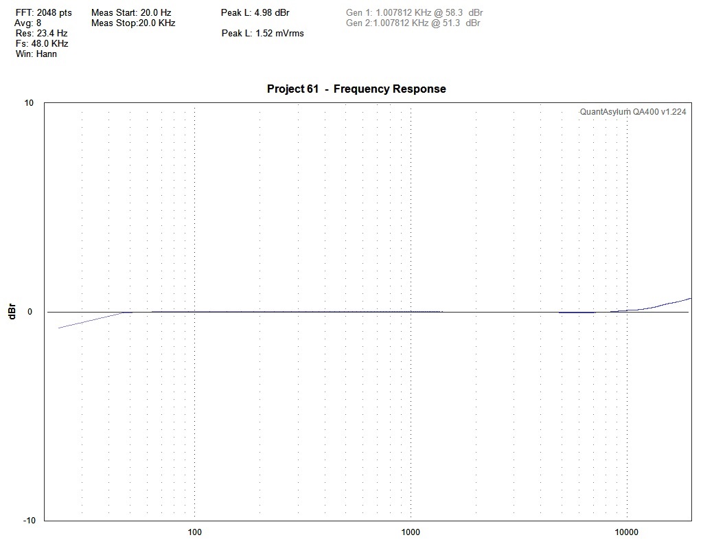
Figure 11. QA400’s Frequency Response test result.
How does Project 61 perform in music listening test? Listening to different CD album genres, the experience was very impressive, as expected. The prototype unit was connected to a modified LM49720 tone control preamp, a Toshiba HD-A2 player, several test speakers and finally into a Bose Acoustimass 3 Speaker System with their inputs paralleled. Listening to Sonny Rollins’ “St. Thomas” from the “Saxophone Colossus” album, you hear well defined lows, extended highs and impressive mids as well, especially on the drum solo. On Keb’ Mo’s HDCD album “Slow Down” especially on the drums and guitars, particularly tracks 3, 6, 8 and 9 you also hear very good musical fidelity.
Here’s something you can tinker or experiment with the completed project; sibilance is improved by adding a 0.01 to 0.1uFD film capacitor across R11.
Update: August 10, 2023
The PCB layout is now at Revision 3, to correct the location of C11. Send your request for the latest
PCB layout (Rev 3) at support@buildaudioamps.com.