Project 30

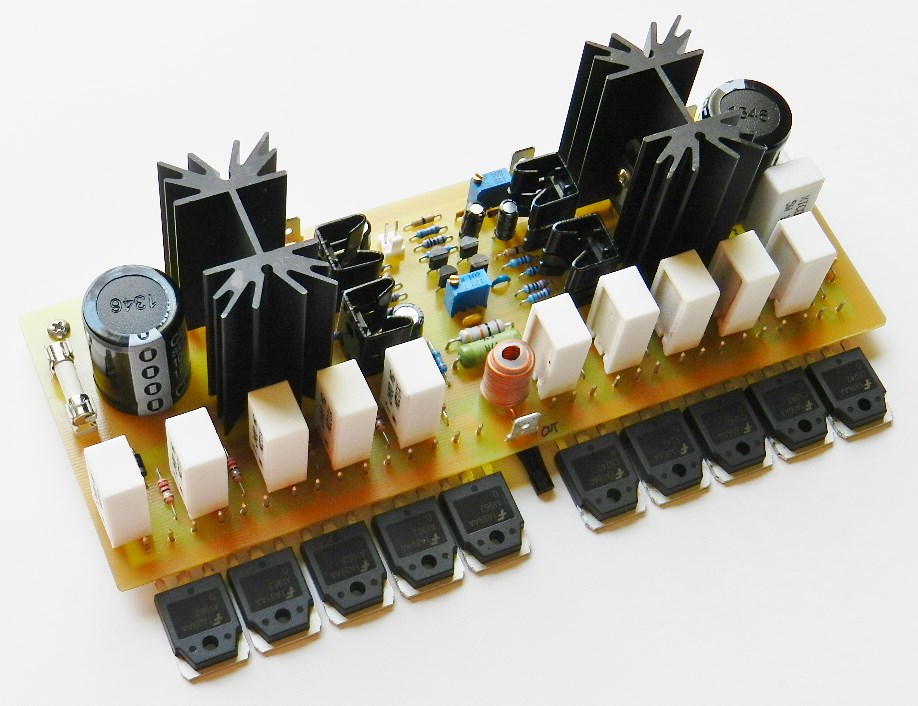
Project 30 is another simple power amplifier project that features a differential voltage amplifier stage and a two-stage emitter-follower output stage. Another feature is the addition of a multi-turn trim potentiometer at the input stage circuit to conveniently adjust the DC offset voltage to zero. The maximum power output of this project before clipping is 213Wrms into an 8Ω load with a ±64VDC to ±75VDC power supply rails.
Here’s a brief description of the circuit:
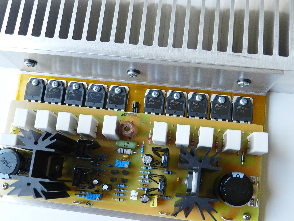
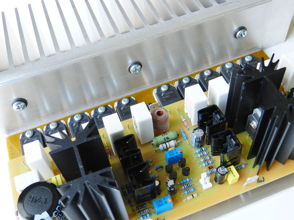
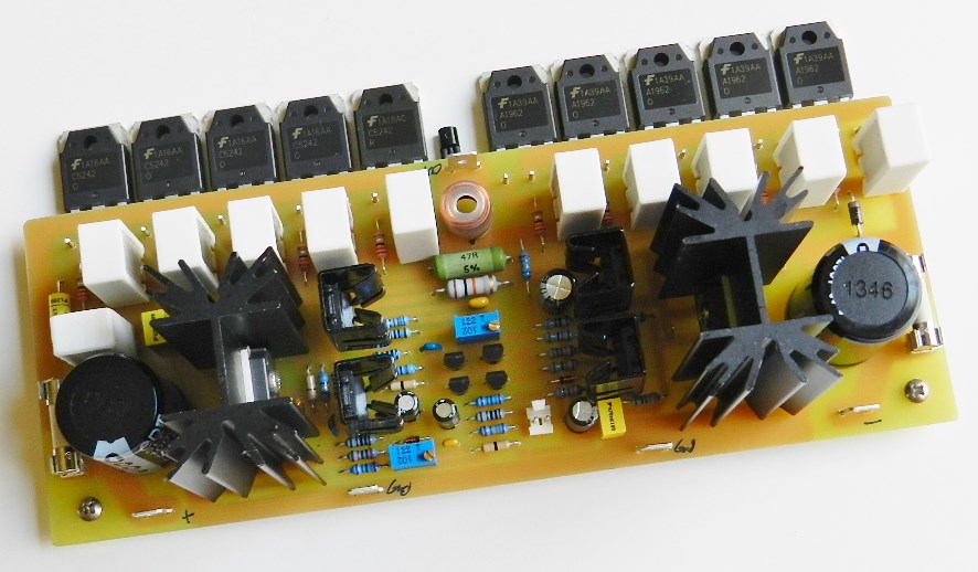
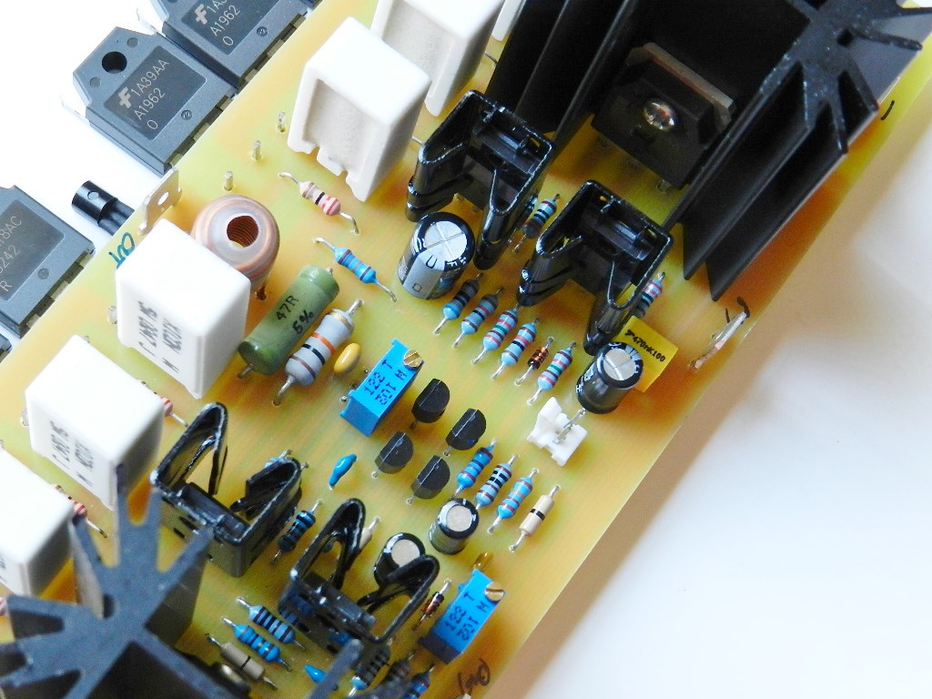
The input signal from J1 passes through a low-pass filter that prevents RF noise from entering the base of Q1. Transistors Q1 and Q2 comprise the input differential amplifier stage current-sourced by transistors, Q3 and Q4. The DC offset voltage can be trimmed within ±10mV by VR1 along with a voltage divider circuit whose mid-point voltage is applied to the base of Q1. R12 and R13 in series with C5 are connected to the base of Q2; these determine the overall gain of the amplifier. The outputs of Q1 and Q2 are connected to the high-gain differential voltage amplifier stage transistors, Q5 and Q6, whose collectors are loaded with current-source transistors Q7 and Q8. Q21 along with VR2 sets the bias of the power output transistors. The emitter-follower configured power transistors Q9 and Q10 drive the power output transistors Q11 through Q20. L1 in parallel with R44 of SMT-type and R43 in series with C11 in the output assure the amplifier’s stability for any connected loads.
If you are interested in building this project and have read the Information and Policies section of this website, the schematic diagram, PCB layout (available by request) and BOM are free, as is, no warranty.
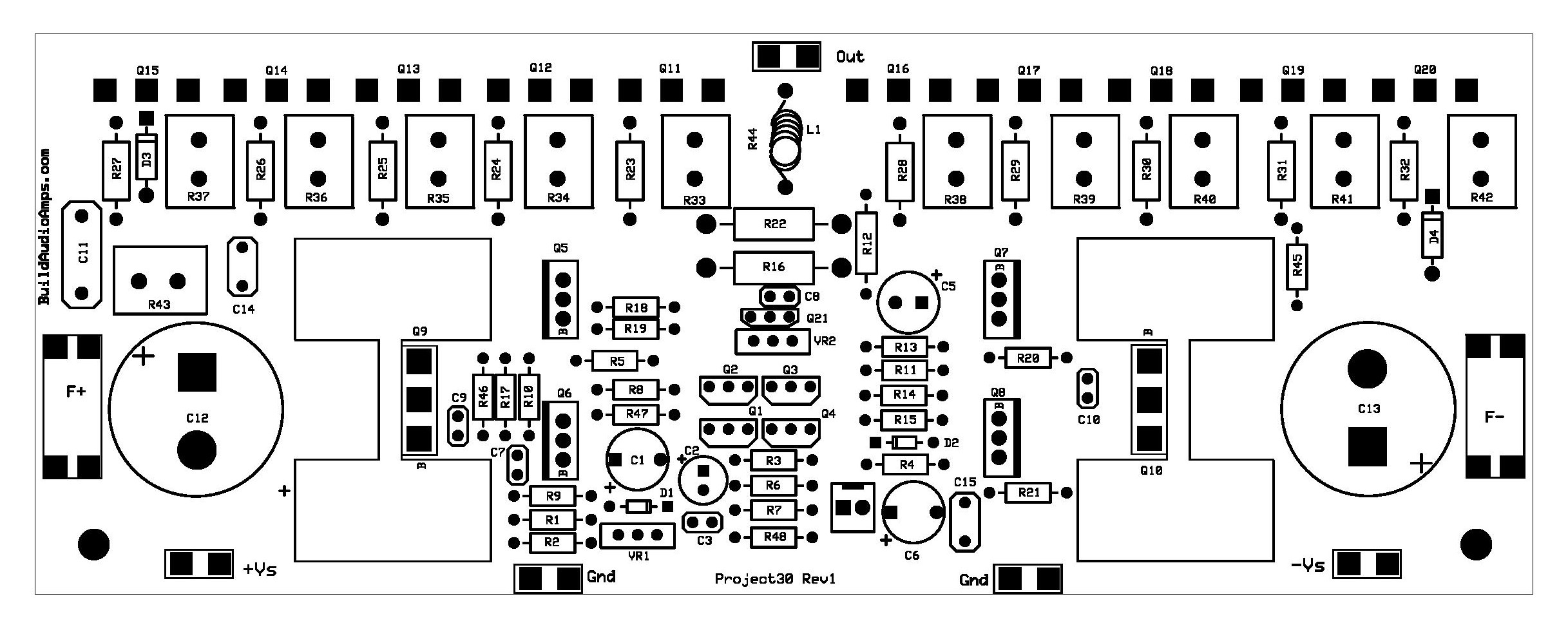
Silkscreen parts placement layer of PCB for Project 30.
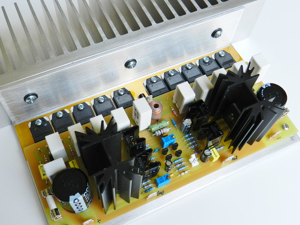
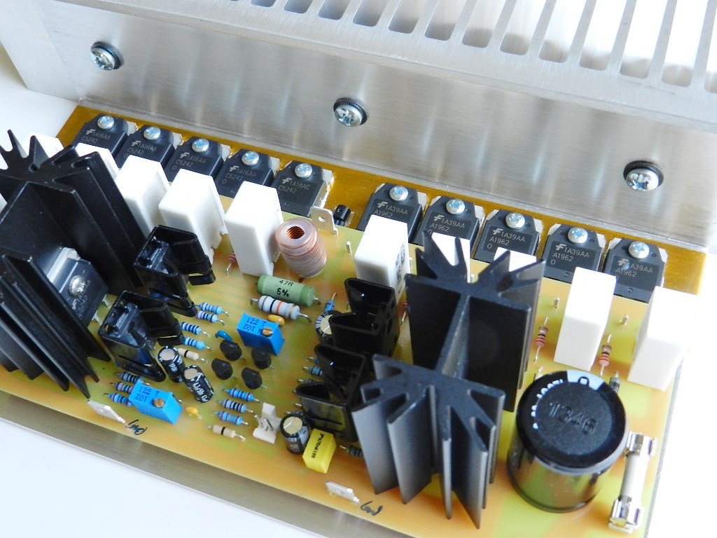
If you’ve decided to build this project and have completed the PCB assembly, the DC offset voltage and bias of the power output transistors need to be adjusted first. The recommended power supply for this project is from ±64VDC to ±75VDC at 3A to 6A. Make sure that power supply has been properly built and its output rails measured before connecting it into the amplifier. Install a shunt or short at the input of the amplifier. Adjust VR2 to its maximum resistance of 1KΩ. VR2 can be accessed on top of PCB at R19 (right end) and base of Q10, please refer to the schematic diagram. Connect an 8Ω dummy load at the output of the amplifier. If you’re installing the project’s PCB similar to what is shown in the next pictures, make sure that the collectors of all power transistors have high or infinite resistance to the metal bracket or heatsink. Q21 is wired and mounted off the PCB with a small piece of double-sided thermal tape similar to the ones used for attaching a heatsink to the CPU, GPU or RAM in computers.
The minimum power supply voltage needed by the amplifier to be able to reproduce any source signals without perceived distortion is ±45VDC. Just to be on the safe side you may consider using a ±45VDC power supply, if available, to initially power the newly built project for testing.
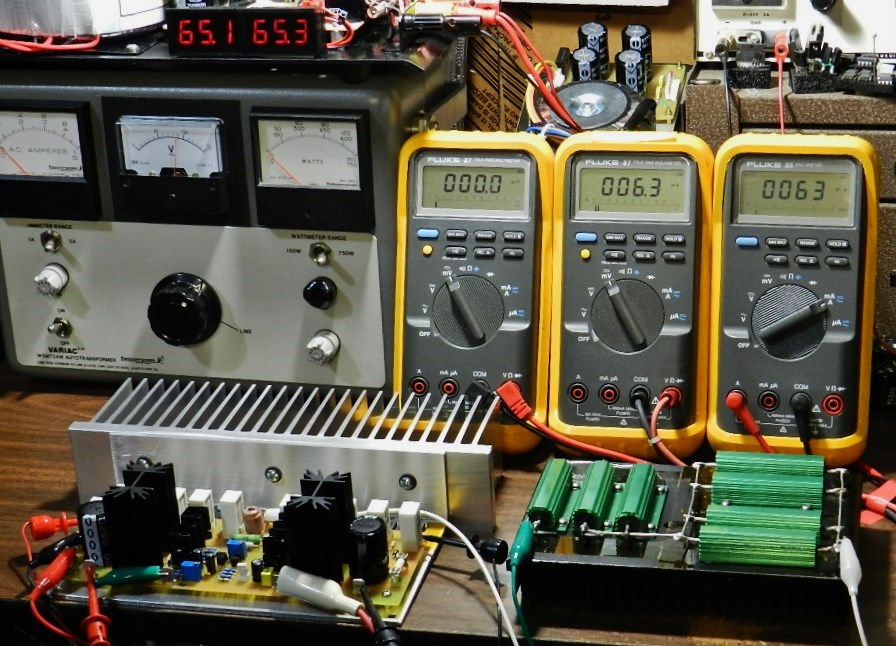
The picture above shows several test clips to temporarily connect the power supply to the amplifier for testing as well as the test probes of the 3 DMMs. Seasoned amp builders have more than 3 DMMs. The DMM on the left side of the picture is reading 0.0mV, the DC offset of the amplifier and this can be adjusted by VR1 within ±10mV. The DMM in the middle is reading 6.3mV, the voltage drop across R37 and R42. Initially it should measure less than 1mV, if not power OFF immediately and check to PCB for assembly errors. The black test probe of the DMM is connected to the emitter of Q20 and the red test probe at the emitter of Q15. Adjust VR2 to get to this value and it could be anywhere between 5mV to 10mV after a warm-up period of 10 minutes. The DMM on the right side of the picture is reading the current across the F+ fuse terminals at 63mA. This reading is dependent on the adjustment of VR2. If you obtained different DMM readings than mentioned, switch the power supply to OFF immediately before any of the populated components vaporize and check the PCB for assembly errors. If not, you may proceed with music test. This project was mated with Project 9 the LM1036 tone control project.

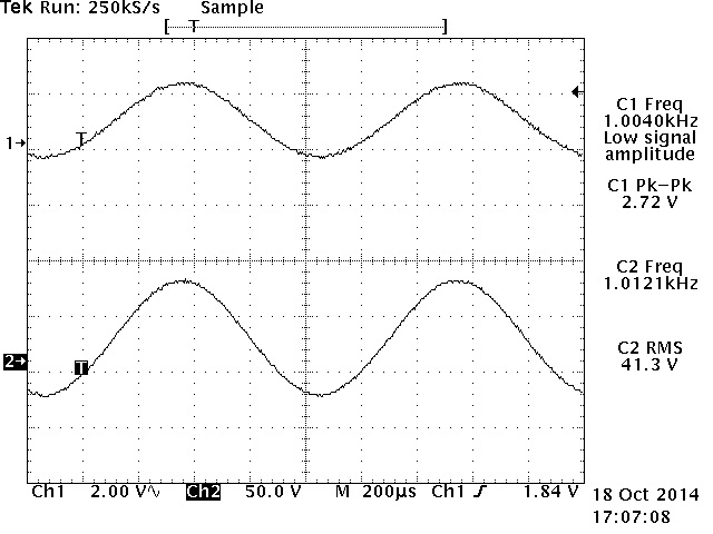
The next test is optional, but if an oscilloscope, function generator and a high-wattage 8Ω dummy load are available, the maximum power output of the amplifier can be measured before clipping occurs. Be careful not to touch the heat sink or the dummy load during the test, they will get extremely hot! The function generator was set for a sine wave output of 1KHz at 2.72Vp-p and connected directly to J1, as well as CH1 probe of the oscilloscope. An 8Ω/700watt dummy load was connected at the output of the amplifier as well as CH2 probe of the oscilloscope. The amplifier produces 41.3Vrms across the 8Ω/700W dummy load for a power output of 213 watts or more than 400 watts into a 4Ω load, as shown in the Tek hardcopy picture above. The scope’s horizontal scale was adjusted at 200uS to verify for any signs of clipping or artifact in both peaks of the output waveform.