Project 23
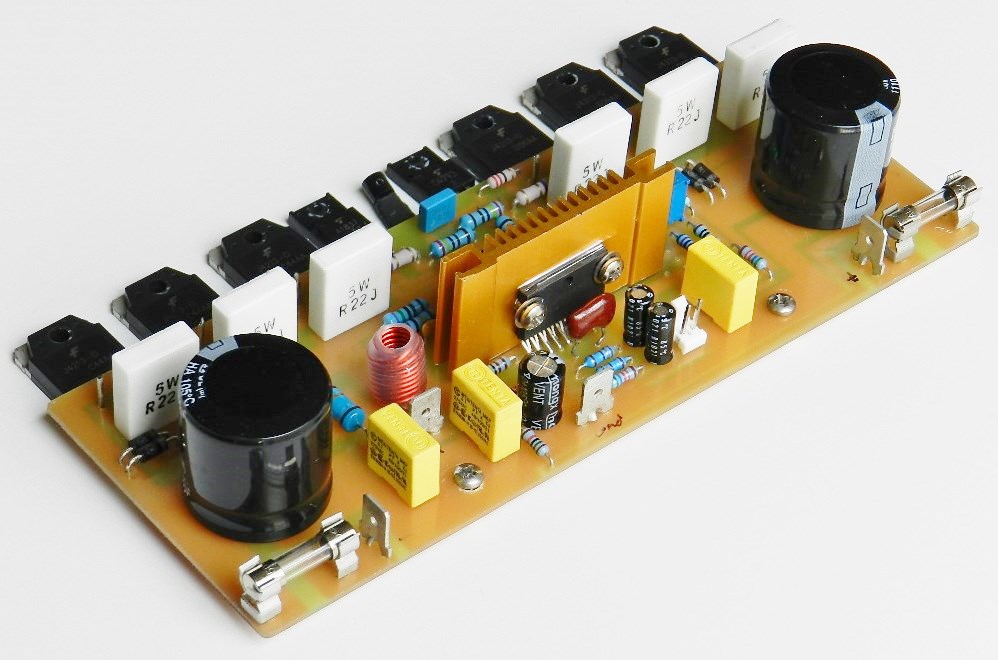
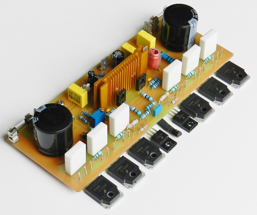
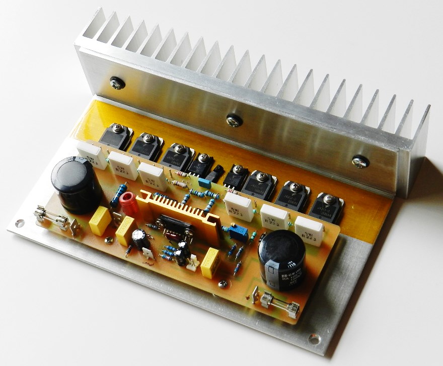
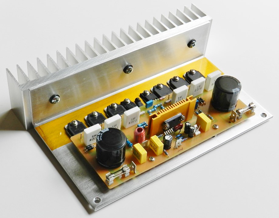
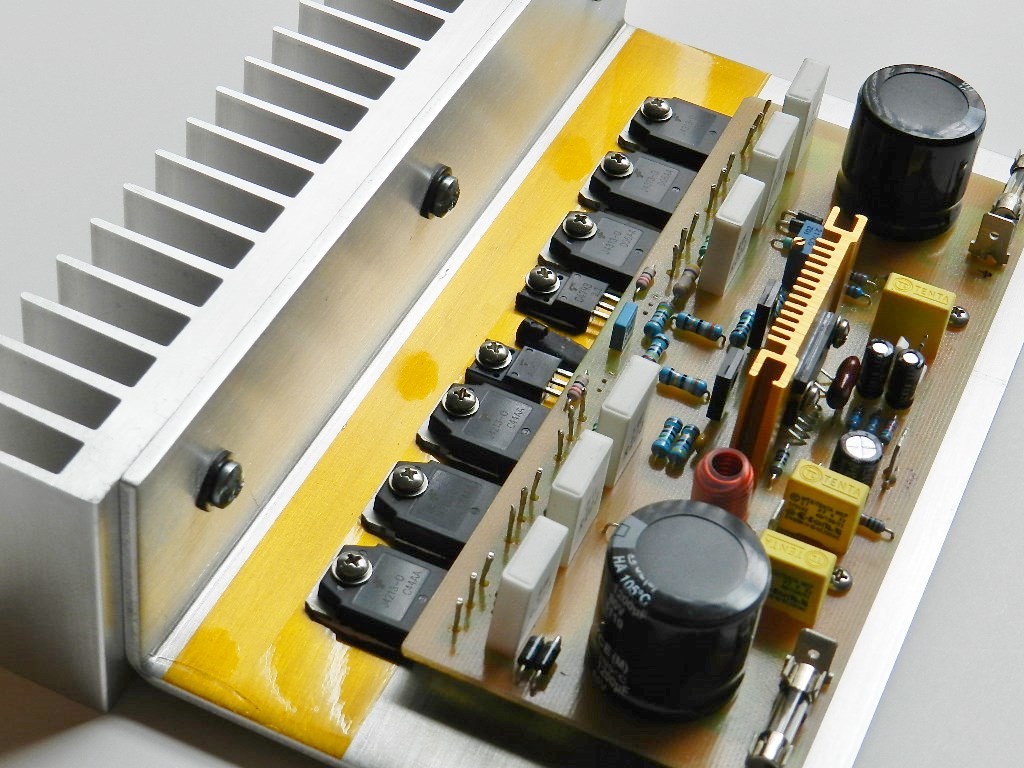
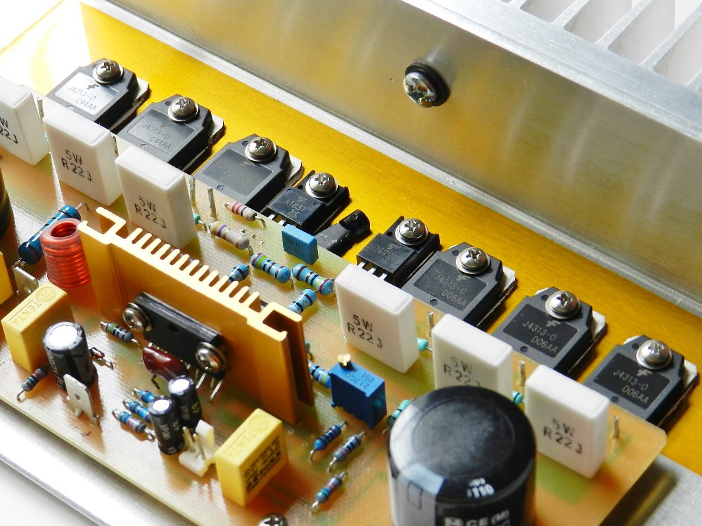
Project 23 uses a unique 2-stage emitter-follower drivers, Q2~Q5, with their emitter resistors R17, R18, R23 and R24 connected to the power supply rails, similar to Project 3. The driver stage circuit is unusual when compared to the most common type, where the emitter resistors are tied to the output of the amplifier or when compared to a T-circuit where the emitter resistor is shared by both NPN and PNP transistors. When Project 23’s drivers are combined with three complementary pairs of paralleled TO-3P packaged power transistors it forms into a familiar 3-stage emitter-follower output stage providing large amount of current to drive the loudspeaker loads.
The measured power output of this project is 128Wrms into an 8Ω load or 256Wrms at 4Ω load. The project can be powered with a ±50VDC up to ±60VDC power supply. Small heat sinks, as noted in the BOM, have to be attached into the TO-126 drivers to improve heat dissipation. The schematic diagrams, BOM and PCB layout for Project 23 are available for free by request, as is, no warranty.
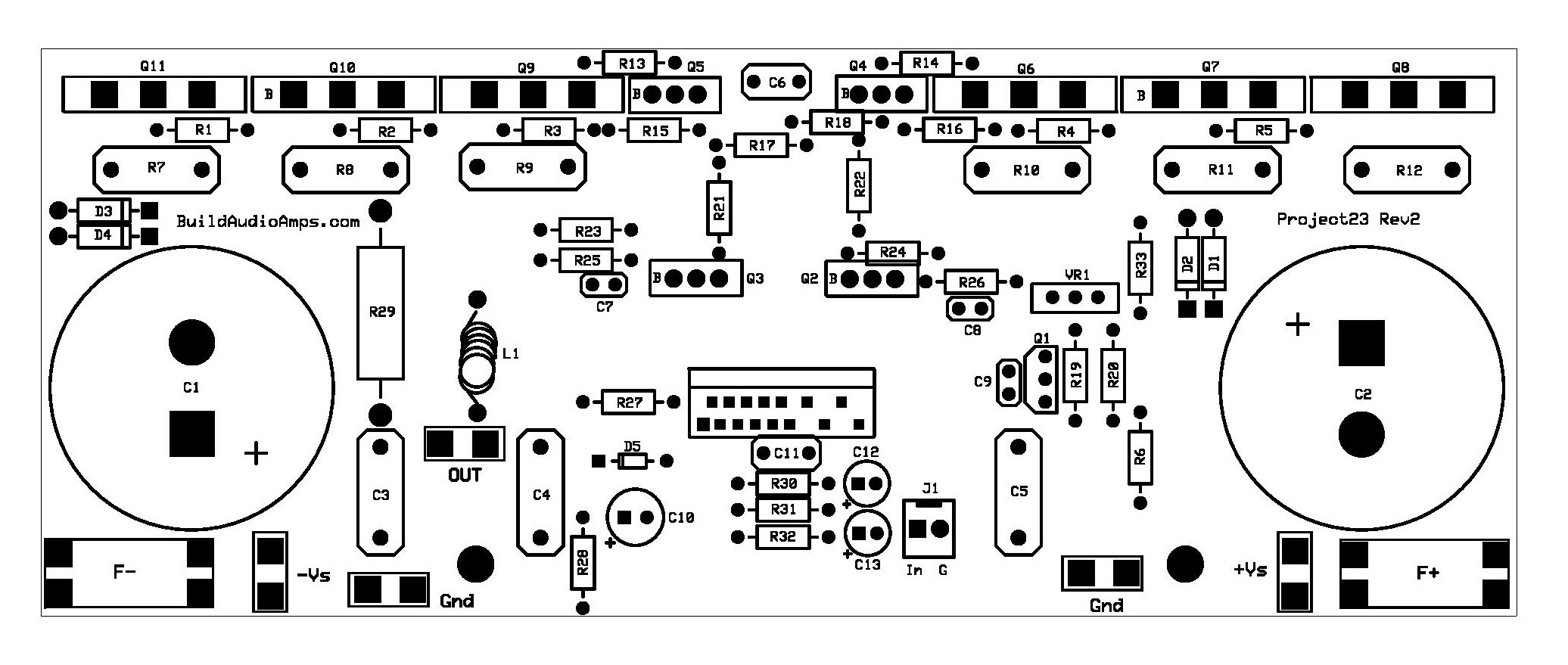 Project 23 Silkscreen parts placement layer of PCB.

It is highly recommended to power a newly built audio amplifier project about half or less of the required power supply voltage rails. Doing so will eliminate most of the disappointment involved when the unexpected happens to the project powered with high power supply voltage rails. Similar to previous projects, I’ve always used and would recommend a +/-24VDC power supply to initially power the amplifier for testing.
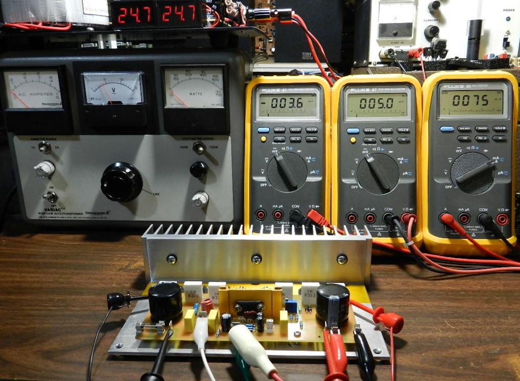
Here’s the fun part! Insert a jumper or shunt at the input of the amplifier. Do not connect any load or loudspeaker at the output of the amplifier. Adjust VR1 for minimum resistance. Prepare 3 DMMs to measure the DC offset voltage, the voltage between the emitters of Q8 and Q11 power output transistors and the current across the F+ fuse terminals.
The picture on the left with a ±24VDC power supply shows the DC offset voltage at 3.6mV measured at the output of the amplifier, 5mV across the emitters of Q8 and Q11 and the current measured across the F+ fuse terminals at 75mA. Gradually adjust VR1 to obtain the 5mV reading after a warm-up period of about 10 minutes. If you get different DMM readings, switch the power supply to OFF immediately and check for PCB assembly errors.
If a Variac transformer is available, connect the AC input of the power supply to the output of the Variac transformer. Switch the power to ON and gradually adjust the Variac’s AC output voltage from zero until the voltage output of the power supply reaches ±50VDC while keeping an eye on sudden increase in any DMM readings. If you have observed an increase in any of the DMM readings, switch the power to OFF immediately and check for PCB assembly errors. The picture on the right with a ±50VDC power supply shows the DC offset voltage at 2.9mV, the voltage across Q8 and Q11 at 5mV and the current across the F+ fuse terminals at 108mA. Readjust VR1 to get the 5mV reading after 10 minutes, after that, you may proceed with music test!
If a Variac transformer is unavailable, make sure that the power supply has been properly built and that the output voltage rails have been measured at ±50VDC up to ±60VDC before connecting it to the project. With the power supply at OFF, adjust VR1 for minimum resistance. Switch the power supply to ON; the DMM measuring the voltage across Q8 and Q11 should read less than 1mV. If the DMM reading is more than 1mV and cannot be adjusted, power OFF immediately and check for PCB assembly errors. If the DMM reading is less than 1mV, wait for 10 minutes for the bias to stabilize and then carefully adjust the reading to 5mV.

The next test procedure is optional, but if an oscilloscope, audio signal generator and 8Ω dummy load are available, the maximum power output before clipping occurs can be measured. Do not touch the heat sink or the dummy load during this test; they will get extremely hot!
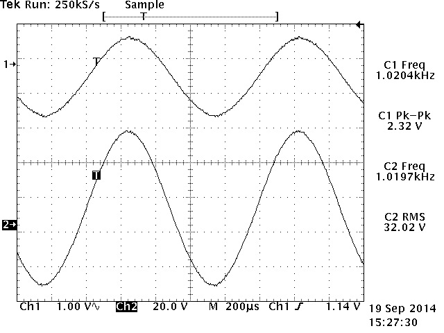
The power output was measured using an HP3312A Function Generator set at 1KHz 2.32Vp-p sine wave output and connected directly to the input of the amplifier under test as well as the CH1 test probe of the oscilloscope. An 8Ω/700Watt dummy load was connected at the output of the amplifier under test as well as the CH2 test probe of the Tektronix TDS520D 500MHz Digital Phosphor Oscilloscope. The amplifier produces 32.02Vrms across the 8Ω/700W dummy load or a power output of about 128Wrms, as shown in the TEK hardcopy picture on the right. The oscilloscope’s horizontal scale was adjusted at 200uS to verify for any visible clipping on its peaks. Project 23 was paired with the LM1036 tone control project and the sound quality it reproduced did not disappoint!